


Raman Mapping of Layer Number, Strain, and Structural Defects in Graphene
Investigating structural defects in graphene can help to determine how structural imperfections can impact the properties of the material. Raman mapping can be used to determine not only structural defects but layer number and strain in a sample, allowing a deeper understanding of how its structure can influence its applications.
Key Points
- The Edinburgh Instruments RM5 Raman Microscope is ideal for mapping the electrical and mechanical material properties of graphene.
- Layer number can be mapped using the G and 2D band intensity ratio.
- Strain maps can be created using the intensity and peak positions of the G and 2D bands.
- Defects can be mapped using the D and G band intensity ratio.
Introduction
Since its theoretical prediction in the 1940s and experimental isolation from graphite in 2004, graphene has rapidly emerged as a highly desirable quantum material in various application areas, including semiconductors, bioengineering, microelectronics, batteries, and composites.1,2 Producing large-scale, defect-free, layer-uniform graphene devices is crucial for many applications. Pristine monolayer graphene exhibits excellent mechanical, thermal, and electronic properties that change with increasing layer numbers, strain, and defects.3 Methods to probe uniformity across graphene devices are therefore crucial for quality assurance.
The Edinburgh Instruments RM5 Confocal Raman Microscope is ideal for analysing graphene. Raman mapping reveals information on graphene’s structural and electronic properties. It can map the location of structural defects, strain, doping, and layer stacking using the relative intensities and positions of the Raman bands in the graphene spectrum, Figure 1. In this Application Note, the capability of the RM5 and Ramacle® software for graphene analysis is demonstrated by mapping the layer number, strain, and defects on graphene films.
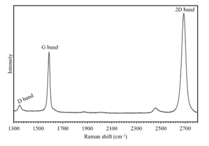
Figure 1. Raman spectrum of graphene with the common modes used for mapping labelled. The D band ca. 1350 cm-1 is a ring breathing mode of the sp2 carbon ring and is Raman active in defective graphene, the G band ca. 1585 cm-1 is caused by an in-plane stretching vibrational mode of the sp2 bonds, and the 2D band ca. 2680 cm-1 originates from a double resonance enhanced two-phonon lateral vibrational process.
Materials and Methods for Investigating Structural Defects in Graphene
The samples analysed were monolayer and bilayer graphene films deposited on Si substrates. Raman mapping was performed on the samples using an Edinburgh equipped with a 532 nm laser, a 100X 0.9 NA objective, and a CCD detector, Figure 2. All mapping data was analysed and plotted using the RM5’s Ramacle software package.
Figure 2. Edinburgh Instruments RM5 Raman Microscope.
Layer Number: Ratiometric Mapping of G and 2D Bands
The variation in layer number across a graphene sample can be determined from the relative peak intensities of the G band (IG) and the 2D band (I2D) in the Raman spectrum.5 As the number of layers in graphene increases, IG increases relative to I2D.6 The 2D/G band ratio (I2D/IG), therefore, can map the uniformity and layer number across graphene flakes and films.
A nominally bilayer graphene sample was mapped using the RM5. Maps of IG, I2D, and the peak ratio I2D/IG were plotted in Ramacle and are shown in Figure 3. The I2D/IG peak ratio varies significantly across the map between 0.1 and 2 (Figure 3c), indicating a significant layer number variation across the graphene sample. Monolayer graphene is typically characterised by an I2D/IG of ≥ 2, while in bilayer graphene, I2D/IG approaches 1. Additional graphene layers cause I2D/IG values to be lower than 1.7,8. Therefore, the black areas (high I2D/IG) on the map were assigned as monolayer graphene, the purple layers as bilayer, and the areas in yellow (low I2D/IG) were assigned as multilayer graphene. The spectra in Figure 3d show the significant change in I2D/IG in the spectra collected within the different regions.
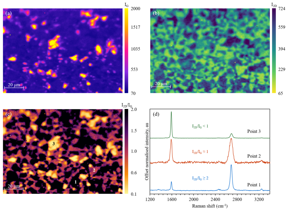
Figure 3. I2D/IG Raman mapping of graphene for layer number determination.
Strain: Peak Position Mapping of G and 2D Bands
Strain in materials causes bond lengths to change, altering their vibrational frequencies and the properties of the material under investigation. Raman spectroscopy is, therefore, highly sensitive to strain. In graphene, strain is associated with frequency changes in the vibrational modes. This is reflected in the Raman shift of the G and 2D bands, meaning the position of these bands can be used to create a strain map of the graphene surface.7
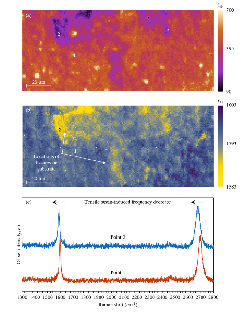 Figure 4. Peak position Raman mapping of graphene for strain detection.
A monolayer film grown on a Si wafer containing several fissures was mapped to track strain in graphene using Raman microscopy, Figure 4. The area mapped on the sample covered two fissures in the Si substrate, which were hypothesised to affect the mechanical properties of the graphene film deposited on top and induce strain. A peak position image for the G band was constructed, Figure 4b and this clearly showed a decrease in the band frequency in the regions where the graphene lay atop the fissures. The reduction in the G band frequency can be assigned to tensile stress in the graphene layer. Tensile stress elongates the graphene sheet, which lowers the vibrational mode energies, resulting in a shift to lower wavenumbers. Spectra from strained and unstrained regions are shown in Figure 4c, where it can also be seen that the frequency of the 2D band decreases in the strained graphene.
The frequency decrease of the G band in Figure 4b could also be caused by an increase in graphene layer numbers. However, IG would increase with increasing layer number, and Figure 4a shows that areas with a G band frequency decrease also have a reduced IG. Therefore, it can be concluded that the peak shifts are due to strain and not layer number. Interestingly, the intensity map also shows regions of high IG, shaded in cream, which could be assigned as multilayer graphene.
Defects: Ratiometric Mapping of D and G Bands
Raman microscopy can track defects on graphene samples because disorder in the lattice creates D and D’ Raman peaks ca. 1350 cm-1 and 1640 cm-1, which would otherwise be Raman-forbidden. These are allowed in spectra of defective graphene because the defect provides the missing momentum to satisfy conservation in the Raman scattering process.8 The number and nature of defects in graphene can significantly affect the performance, which can either be detrimental or advantageous depending on the intended application of the material. For example, defects have been shown to diminish electron mobility on graphene deposited on substrates, but they have also been reported to enhance the reactivity of graphene-based catalysts.9,10
The graphene sample was mapped on the RM5 and ID and IG were initially plotted in Ramacle, Figure 5a and b. ID/IG was subsequently plotted in Ramacle, and the resulting image is shown in Figure 5c. ID/IG is a valuable metric for determining pristine and defect-dense graphene regions on a sample. In pristine graphene, this ratio is typically close to 0, and as the defect density increases, the ratio will increase. In Figure 5c, the dark blue regions were assigned as low-defect-density graphene, and the areas shaded in red and yellow were high-defect-density graphene. Spectra from different regions of the map are shown in Figure 5d.
In the high-defect-density region, the D band is more intense than the G band, whereas in the low-defect-density region, the G band is dominant, and no D band is visible. The D’ band is also present in the defect-dense regions and appears as a higher-Raman shift shoulder of the G band. The ratio between the D and D’ bands can also be used to discriminate between different defect types; for example, a larger value is associated with sp3-type defects and lower values are associated with vacancy-type defects.8
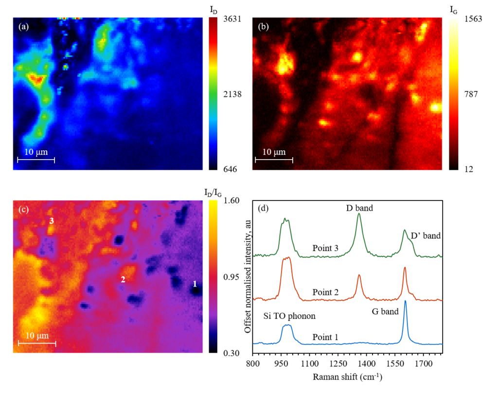
Figure 5. ID/IG Raman mapping of graphene for defect detection.
Conclusion
An Edinburgh Instruments RM5 Confocal Raman Microscope was used to map layer number, strain, and defect density in graphene films. The RM5 is ideal for full analysis graphene, including investigating structural defects in graphene, revealing a wealth of information about the structural and electronic properties of the graphene layer with high sensitivity and spatial resolution.
