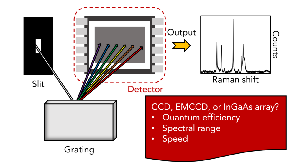
Unsure whether a CCD, EMCCD, or InGaAs detector is best for your Raman application? In this Spectral School tutorial, we discuss the differences between the detectors available for Raman microscopes, and how to select one based on important performance parameters such as quantum efficiency and spectral range.
In a Raman microscope, the role of the detector is to convert photons into a meaningful signal that provides qualitative and quantitative information about the molecular structure of the sample under investigation. Several types of detectors are available, and they can all be evaluated in terms of their sensitivity to incident photons and the spectral range over which they are operational. An ideal detector would convert every photon to an output signal, but in practice, the functionality of a detector is typically limited to a specific spectral region that is dictated by its constituent materials and the manufacturing process. Since Raman spectroscopy can be applied to an extensive range of samples with widely varying optical properties, the consideration and careful selection of a detector before commencing a research project are vital to the optimisation of later results. In this Spectral School tutorial, we will discuss the different types of detectors available for Raman microscopes and how the sensitivity and spectral range required by the user will dictate their choice of detector.
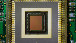
Raman microscopes most commonly contain charged-coupled device (CCD) detectors and are very sensitive to photon detection. A CCD is a silicon-based multi-channel one- or two-dimensional array detector that is capable of quickly detecting whole spectra. Each channel within the CCD is a photodiode pixel, of which there are several thousand, and generates electronic charge proportionally to the number of absorbing photons. Therefore, the more photons that reach a CCD pixel in a given time frame, or the longer the photons are allowed to impact the pixel, the more charge is built up and the larger the signal detected. The simplest type of CCD is a full-frame CCD, Figure 1, in which the incoming photons are absorbed on a fully light-sensitive array and the built-up charge is shifted vertically to a readout register before being shifted horizontally to a charge amplifier. Here, the charge is converted to voltage for readout, and at the end of this process, the output can be displayed as a spectral signal on a computer. In a Raman spectrometer, the diffraction grating disperses the scattered light onto the longitudinal axis of the CCD array, meaning that an entire spectrum can be detected in a single acquisition. In two-dimensional CCD arrays, each column corresponds to a wavelength and all of the charges from each pixel in a column are accumulated.

Figure 1. The structure of a CCD.
The ability of a CCD to detect a photon is characterised by a parameter called quantum efficiency (QE), which is a ratio between the number of electrons generated and the number of photons absorbed and is a key indicator of detector sensitivity. The QE of a detector varies with wavelength, and the result of a plot of the two variables is a QE curve that characterises the performance of the detector across its operational wavelength range, Figure 2. Each detector has a unique QE curve, which means that the sensitivity and spectral range of different detectors can easily be compared and evaluated with respect to the user’s research requirements.

Figure 2. Example of a QE curve for a CCD detector.
Despite being very sensitive to photon detection, CCDs are limited in applications involving small numbers of photons because they cannot deliver both high sensitivity and rapid acquisition speeds simultaneously. This is because, in a CCD, readout noise scales with the speed at which the charge is amplified, which reduces the sensitivity of detection. This is especially noticeable when using samples that have small Raman scattering cross sections, are low in concentration, or require very fast spectral acquisition times. Electron-multiplied CCDs (EMCCDs) are an alternative type of detector without this limitation and hence they offer ultrahigh sensitivity and speeds. EMCCDs utilise a frame-transfer CCD structure in which the photons are captured in an image section and the resulting charge is temporarily stored in a parallel storage section. Crucially, they are also equipped with multiplication gain technology to increase the number of electrons generated from a single photon, Figure 3. This occurs before the charge reaches the charge amplifier, so the signal is boosted significantly in comparison to noise. They are the best option for fast mapping or for imaging samples that have low levels of Raman scattering.

Figure 3. The structure of an EMCCD.
In an EMCCD, electrons generated from the absorption of photons in the depletion region are accelerated along a multiplication register when voltage is applied. Secondary electrons are generated via impact-ionisation processes in the multiplication register, and the number of electrons produced increases exponentially with voltage. This increase in electrons can be modelled as a function of the number of pixels on the multiplication register and the probability that an electron within each pixel will create a second electron:
G = (1+P)N
Here, G is the gain, P is the probability of gain occurring and it ranges between 0.01 and 0.016 depending on the voltage applied and the temperature of the detector, and finally, N is the number of pixels. It should also be noted an EMCCD can be operated with adjusted gain levels and even without gain, as is shown in the example spectra in Figure 4, in which case it would compare in performance to a standard CCD.
 Figure 4. Raman signal increase triggered by multiplication gain.
The two types of CCDs and EMCCDs available are front-illuminated (FI) and back-illuminated (BI), named in terms of the direction incident photons interact with the detector. These detectors differ significantly in their structures, and therefore they have very different QE curves. As can be observed in the example QE plots in Figure 5, a BI CCD offers a higher QE and hence sensitivity than a FI CCD across the entire range that the silicon is photoactive.
 Figure 5. Quantum efficiency plot for silicon BI and FI CCDs.
In FI CCDs, incoming light passes through electrode structures and insulating layers located in front of the photosensitive silicon depletion region in which photons are converted into electron-hole pairs to generate charge, Figure 6. The electrodes and insulating layers absorb and reflect a portion of the incoming photons before they reach the silicon, and therefore reduce the QE, which reaches a maximum of between 50% and 60%. This absorbing region is impenetrable to photons with wavelengths of less than 400 nm, which means that standard FI CCDs cannot be used for UV Raman applications.

Figure 6. FI CCD detector structure.
BI CCDs, also referred to as back-thinned CCDs, are designed to have improved QE by overcoming the photon flux losses encountered when using FI CCDs. BI CCDs are configured in a process that allows direct exposure of the active photosensitive silicon depletion region to the incoming photons, Figure 7, and therefore they exhibit much higher QEs from the UV to the NIR that reach up to 95%. Although they are not obscured from incoming light by UV-absorbing wires and electrodes, UV photons are absorbed in the surface layers of the semiconductor and are unable to penetrate deeply into the depletion region, which is why the QE of standard BI CCDs decreases at lower wavelengths.

Figure 7. BI CCD detector structure.
Despite the enhancement in QE offered by BI CCDs over FI CCDs, they are prone to significant signal modulation in the NIR caused by constructive and destructive optical interference known as etaloning, Figure 8. This effect was coined because the behaviour described is analogous to a type of interferometer called a Fabry-Pérot étalon.
 Figure 8. Etaloning effect in BI and FI CCDs when using a 785 nm laser to analyse a silicon wafer.
The penetration depth of light in the photosensitive silicon increases with wavelength, to the point where the material is semi-transparent in the NIR, and the consequence of this is that NIR light can propagate through large thicknesses before being absorbed. This penetration depth is several times the thickness of the ultrathin photosensitive silicon of the BI CCD, and because there are large refractive index differences and hence reflectivity at both interfaces (insulating layer-silicon and silicon-air) of this region, NIR photons can undergo back-and-forth internal reflection which generates interference, Figure 9A. It is important to note that etaloning will not occur when visible excitation wavelengths are used, but it can become more prominent when 785 nm or longer wavelength excitation sources are used, especially when the sample under investigation is reflective or requires high acquisition times because it is a weak Raman scatterer. FI CCDs do not suffer from this effect, because incident NIR photons are not reflected into the depletion region by a reflective interface. Instead, the photons that are not absorbed in the silicon are lost in an optically dead bulk substrate.
There are several approaches for reducing etaloning in BI CCDs. The first is the application of an anti-reflective (AR) coating to increase the transmissivity of the silicon-air interface, Figure 9B. When NIR photons enter the silicon region in a BI CCD and propagate towards the insulating layer without being absorbed, they will be reflected towards the front surface with the silicon-air interface. If this front surface is AR coated, the number of photons that undergo further internal reflection and contribute to signal modulation in the silicon is reduced. Another approach is to roughen the back surface of the silicon region during the manufacturing process, Figure 9C. This is referred to as fringe suppression and it helps to reduce etaloning because it breaks the parallelism of the two reflective interfaces and thus reduces constructive interference. Finally, the depth of the silicon depletion region can be increased, Figure 9D. The benefit of a deep depletion region is that NIR photons have a higher probability of being absorbed before multiple internal reflections occur. BI CCDs can be manufactured with all three features to reduce interference patterns in spectra and increase QE in the NIR, but it should be noted that etaloning can never be fully removed.

Figure 9. Manufacturing techniques for reducing etaloning in BI CCDs.
Due to the semiconductor materials and the manufacturing processes used to make standard FI and BI CCDs, the QE of both detector types are compromised in the UV region of the electromagnetic spectrum. The insulating region and electrodes that cover the depletion region in FI CCDs are opaque to light with wavelengths less than 400 nm, and the first few surface layers of the depletion region absorb UV light strongly in BI CCDs. Physical and chemical changes are therefore needed to improve the QE of both CCD types at lower wavelengths, such as passivating the semiconductor material to reduce charge-carrier recombination and applying down-conversion coatings on the surface to increase depth penetration. Such enhancements are available for FI and BI CCDs, Figure 10.

Figure 10. Quantum efficiency plot for UV-enhanced CCDs.
The QE of CCDs drops off sharply in the IR and as a result, they cannot be used to detect light with wavelengths greater than 1100 nm. This is because the silicon in the depletion region cannot absorb photons that are lower than its bandgap energy. Spectral detection capabilities can be extended beyond this limit in a Raman spectrometer by using an alternative type of detector based on a material called indium gallium arsenide (InGaAs), a semiconductor alloy of gallium arsenide and indium arsenide that has a lower bandgap energy than silicon and exhibits excellent photosensitivity in the NIR and shortwave IR range. Typically, InGaAs detectors exhibit QEs of above 80% between 1000 nm and 1600 nm and are sensitive up to 1700 nm, Figure 11, greatly outperforming silicon CCDs and making them essential for Raman applications that utilise a 1064 nm laser.
 Figure 11. Quantum efficiency plot for back-illuminated CCDs and InGaAs detectors.
Detectors for Raman spectrometers vary in their sensitivity, spectral range, and cost, and the end user must carefully consider how these parameters will relate to their research needs. Table 1 provides a guide for choosing one of the detectors discussed based on those performance criteria. Selecting the correct detector for a given application will depend on the excitation wavelength needed, the Raman scattering cross-section of the sample, and the desired acquisition time for spectral analysis or imaging.
Table 1. Guide for choosing a detector type for a Raman microscope.