


High-Resolution Raman & Photoluminescence Imaging of MoS2
Introduction
Transition metal dichalcogenides (TMDs) are a class of 2D materials which have unique optical and electronic properties. They are semiconductors with the chemical structure MX2 where M is a transition metal and X a chalcogen, Figure 1. After the isolation of graphene layers, research into alternative 2D layered materials which offer the same, or better, properties has surged.
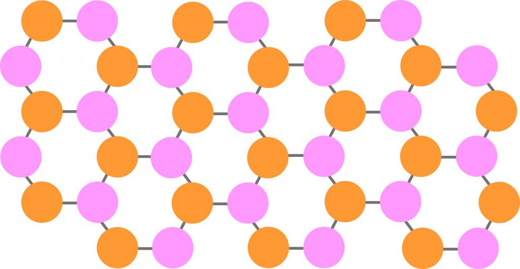
Figure 1: TMD structure MX2; M=Transition Metal (pink) (e.g., Mo) X=Chalcogen (orange) (e.g., S)
Bulk MoS2 has an indirect band gap, while in monolayer form the band gap becomes direct. The direct band gap is formed due to the removal of interlayer interactions meaning electrons are confined to a single plane. Mechanically MoS2 monolayers are highly flexible, they have a higher breaking strength than commonly used flexible plastics, and stiffness comparable to steel.1
The applications of MoS2 are numerous and wide-ranging, with interest from fields such as optoelectronics, water treatment, solar energy, and biomedicine. For the material to perform at its highest capability it must be defect free. Defects, stress, and strain can significantly influence the properties of the material. For example, removing defects responsible for non-radiative recombination allows photoluminescence quantum yields of over 95% to be realised.2 Correlative Raman and photoluminescence (PL) imaging can be used to provide highly detailed sample information without any sample preparation or damage.
Using a confocal Raman microscope both Raman and PL maps can be obtained on the same sample area. In this Application Note, CVD-grown MoS2 flakes are analysed using Raman and PL imaging with the RM5 Raman Microscope.
Materials and Methods
An Edinburgh Instruments RM5 Raman Microscope equipped with a 532 nm laser and two gratings; 300 gr/mm for PL and 1800 gr/mm for Raman, was used to analyse MoS2 flakes. The MoS2 flakes were Chemical Vapor Deposition (CVD) grown on sapphire, Figure 2.
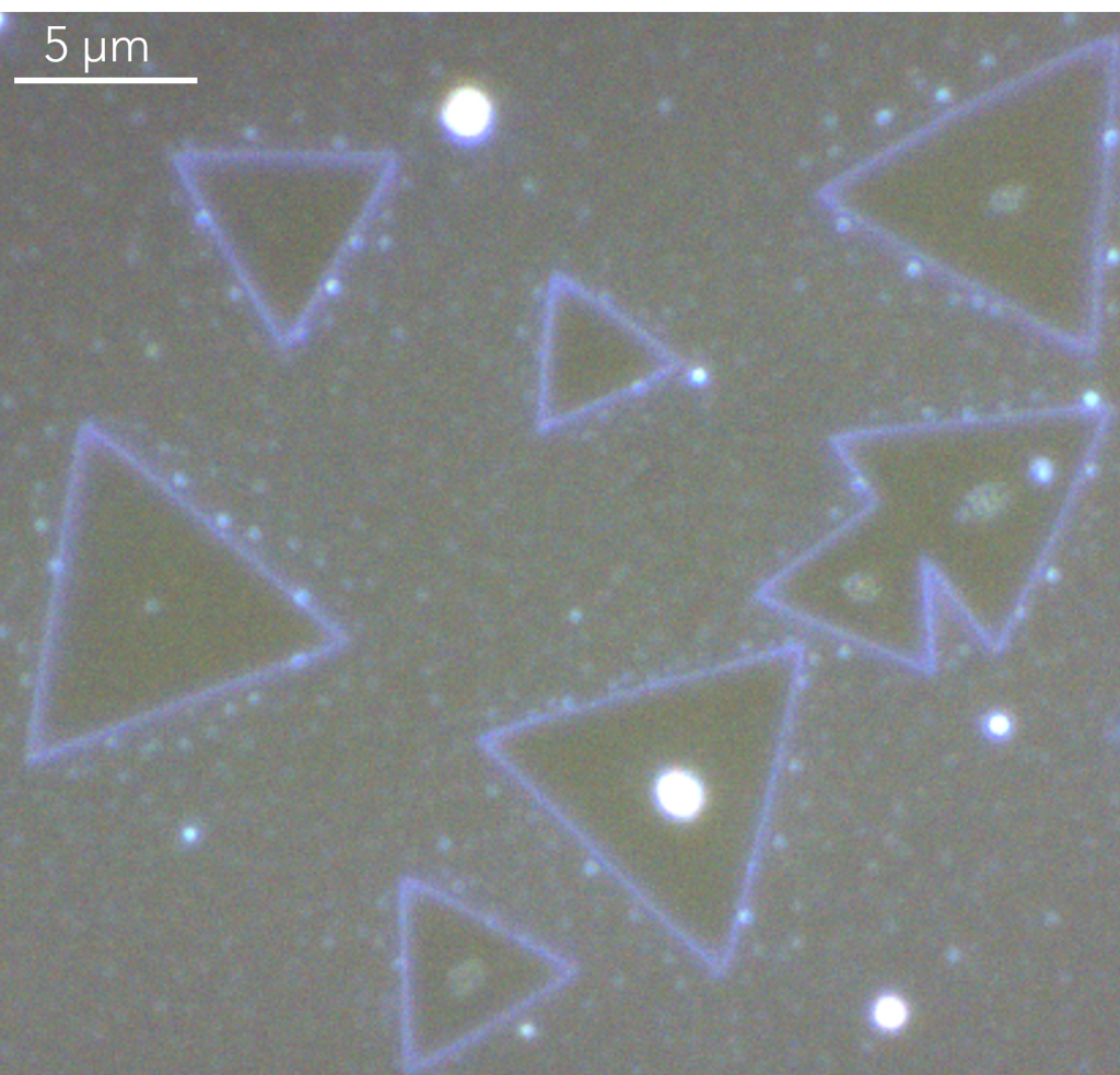
Figure 2: Reflected darkfield image of MoS2 flakes.
The sample exhibits a strong Raman and PL response allowing short exposure times on the CCD camera to be used to obtain high quality spectra. During mapping When exposure times of < 0.5 seconds can be used, Fast Mapping is employed to greatly reduce mapping times. For Raman imaging an exposure time of 0.03 s was used, since PL was more intense 0.01 s exposure times could be used.
MoS2 Raman Imaging
The Raman spectrum of MoS2 consists of two characteristic bands termed the E2g band at 385 cm-1 and the A1g band at 405 cm-1, Figure 3. The E2g band is due to in-plane vibrations, and the A1g band attributed to out-of-plane vibrations.
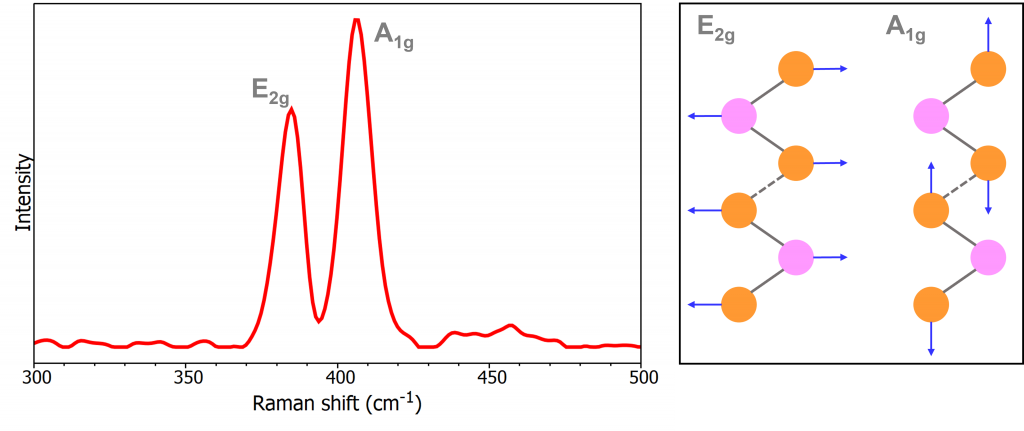
Figure 3: Raman spectrum of thin layer MoS2 (left) highlighting the E2g and A1g bands and their associated vibrations (right).
These bands are indicative of the number of layers present and the number of layers present in MoS2 crystals is critical to their function in optoelectronic devices. From Figure 4 it can be seen the E2g and A1g band intensity are indicative of the number of layers present, as the number of layers increases the two bands become farther apart due to inter-layer vibrations. Crystals shown in a solid single pink colour are monolayer MoS2. While the bright spots in the centre of some of the crystals indicates the presence of multilayer MoS2.
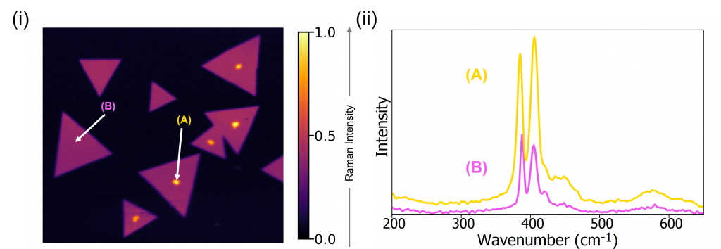
Figure 4: (i) Raman intensity imaging of MoS2 crystals using the E2g and A1g bands. (ii) Raman spectra from areas of low and high Raman signal.
The splitting between the two bands was plotted, Figure 5(i). Compared to bulk MoS2 the E2g band is red shifted as the crystal becomes monolayer, this shift is due to Coulomb interactions between Mo atoms which are enhanced with increased layers.3 The A1g band is blue shifted as the MoS2 becomes monolayer, resulting in the centre of the triangles exhibiting an increased splitting value.
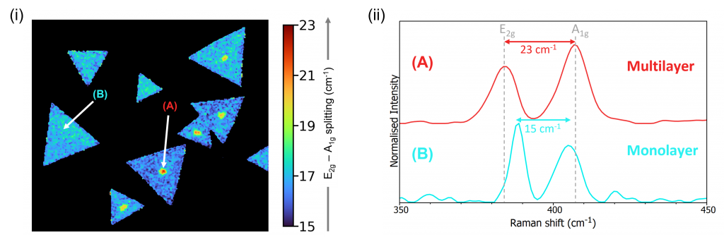
Figure 5: (i) Raman imaging displaying the band splitting of E2g - A1g (ii) Normalised Raman spectra from monolayer and multilayer MoS2 highlighting the change in splitting.
The E2g band is particularly sensitive to strain in the sample, when under strain the band is red shifted revealing the two bottom crystals highlighted in the white box are under more strain than the others, Figure 6. Raman mapping reveals these samples contain both monolayer and multilayer MoS2 whilst showing some strain.
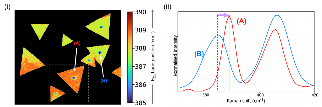
Figure 6: (i) Raman imaging displaying the band position of the E2g band and (ii) Normalised Raman spectra highlighting E2g band position.
MoS2 Photoluminescence Imaging
Excitation using a 532 nm laser offers both Raman and PL signal meaning the two phenomena can be seen in a single spectrum, therefore it is technically possible to perform the two techniques simultaneously. However, to obtain the best quality spectra different gratings are used for the two measurement types. For PL imaging a low groove density grating is used to obtain the broad PL peak. The intensity of the PL band decreases with increasing layer number and bulk MoS2 produces no PL signal at all. This effect is due to the indirect to direct band gap transition which occurs as we go from bulk MoS2 to few-layer MoS2. The Raman and PL intensity maps should therefore be opposites of one another when comparing areas of monolayer and multilayer MoS2 which can be observed in Figure 7.
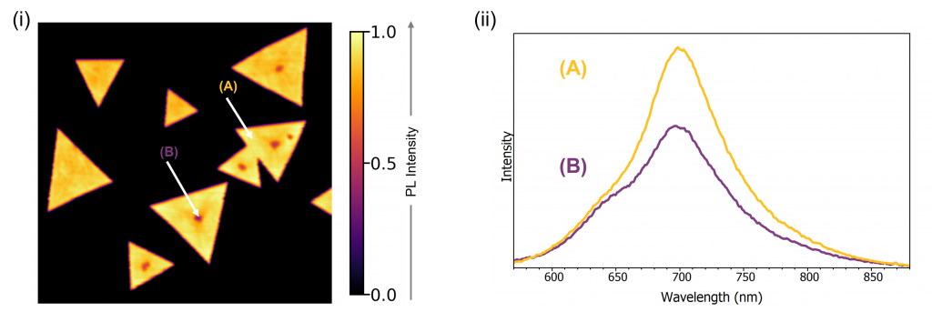
Figure 7: (i) PL intensity map of MoS2 crystals. (ii) PL spectra from an area of high and low intensity.
The PL peak is also sensitive to strain, doping, and defects, its position was plotted in Figure 8. The peak position is indicative of strain in the sample, corresponding with the E2g band from Raman imaging the bottom two crystals reveal strain. Additionally, PL mapping reveals some strain in the two crystals which appear to be growing into each other, highlighted in the white box.
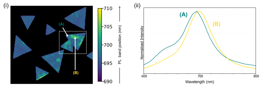
Figure 8: (i) PL imaging of MoS2 crystals using peak position. (ii) Normalised PL spectra from an area of high and low intensity
PL mapping offers agreement with the Raman data showing this sample has been well grown as largely monolayer crystals with little strain present.
Conclusion
This application note demonstrates how the RM5 Raman Microscope can provide high resolution imaging of 2D transition metal dichalcogenides. Raman and PL imaging can be used correlatively to gain detailed information on the sample’s layers, as well as indicating strain, defects, and doping.
References
- J. Pei et al., Exciton and Trion Dynamics in Bilayer MoS2, Small, 11, 6384–6390 (2015)
- M. Amani et al., Near-unity photoluminescence quantum yield in MoS2, Science, 350, 1065–1068 (2015)
- S. Golovynskyiet al., Exciton and trion in few-layer MoS2: Thickness- and temperature-dependent photoluminescence, Appl. Surf. Sci. 515 (2020)
Keep in Touch
If you have enjoyed this application note and would like to be the first to hear the latest product news from Edinburgh Instruments, be sure to sign up to our eNewsletter and follow us on social media using the links below.
