


Photoluminescence and Electroluminescence Confocal Imaging of an OLED
Key Points
- Photoluminescence and electroluminescence are important techniques in the development of organic light-emitting diode (OLED) visual display technology.
- Here, these techniques are coupled with confocal microscopy to image the optoelectronic properties of an OLED device using the RMS1000 Confocal Raman Microscope.
- Spectral and time-resolved imaging reveal much more detailed information about the composition and quality of the device than would be detected with bulk measurements.
Introduction
In recent years organic light-emitting diodes (OLEDs) have become one of the leading technologies for full-colour display panels in high-end smartphones and televisions.1 This rapid growth in use has occurred because OLEDs offer an all-around superior performance to liquid crystal displays (LCDs). For example, they are thinner, lighter, more flexible, less power consumptive, and brighter.2
In a typical OLED device, electrons and holes are injected into organic electron and hole transport layers and they then recombine in a central doped emission layer. The energy generated from this recombination is transferred to a dopant molecule via resonant transfer, and this causes it to emit light. The colour of the OLED emission is governed by the chemical structure of the dopant molecule in the emission layer. When new OLEDs are developed, the optoelectronic properties of individual components and the complete device can be characterised using photoluminescence (PL) and electroluminescence (EL) spectroscopy.
In this Application Note, the RMS1000 Confocal Raman Microscope is used to characterise and spatially resolve the optoelectronic properties of a fabricated OLED device with four imaging modalities: PL, EL, time-resolved PL (TRPL), and time-resolved EL (TREL). Using a confocal microscope to characterise an OLED’s spectral and time-resolved properties provides much greater detail than bulk measurements.
Materials and Methods
A phosphorescent OLED device was prepared by the Organic Semiconductor Optoelectronics group at the University of St Andrews. The sample was placed on an electrical probe stage (LINKAM HFS350EV-PB4) and two tungsten probes were connected to the electrodes on the device to illuminate a single OLED pixel. Spectral and time-resolved PL and EL imaging were performed using an RMS1000 Confocal Raman Microscope, Figure 1.
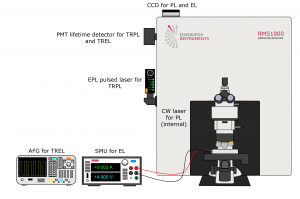
Figure 1. Experimental setup for PL, TRPL, EL, and TREL imaging.
The electrical probe stage containing the sample was placed in the microscope stage insert, Figure 2. For spectral PL measurements, the system was equipped with a 532 nm CW laser and a back-illuminated CCD camera. For TRPL measurements, the system was equipped with an externally coupled EPL-405 picosecond pulsed diode laser, phosphorescence lifetime electronics based on single photon counting multichannel scaling (MCS), and a High-Speed PMT lifetime detector.
For spectral EL measurements, a Keithley 2450 Source Measurement Unit (SMU) was used to apply a bias to the OLED device and electroluminescence detected with the CCD. Finally, for TREL measurements, a Tektronix 31102 Arbitrary Function Generator (AFG) was used to apply a train of short voltage pulses to the OLED. The resulting decay after each pulse was measured using MCS. 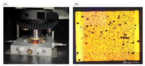
Figure 2. (a) Electrical probe stage fitted on the RMS1000. (b) Widefield view of electroluminescent OLED pixel through the microscope.
Results and Discussion
Large Area Photoluminescence and Electroluminescence Spectral Imaging
The OLED was first investigated using a combination of spectral PL and EL. When combined with imaging using a confocal microscope, these techniques can reveal information about the distribution of the optically relevant materials throughout the device and the device’s overall quality in terms of the uniformity of the emission intensity and colour. The PL image and corresponding spectra in Figure 3 provide information about the distribution of the emissive layer throughout a 4-pixel area on the device, and the location of the electrodes are also shown for reference.
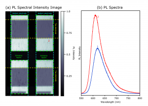
Figure 3. (a) Spectral PL image of OLED device. (b) PL spectra from points 1 and 2 labelled in the image in (a).
The white (highest) and grey (reduced) PL intensity regions, bordered collectively in green, show the location of the organic emissive layers in the four pixels. The grey regions were determined to be the locations at which the emissive layer were covered by the top electrodes. This is because, where the top electrode crosses the emissive layer, the PL emission is reduced to less than half the intensity of the uncovered areas. This is due to the top electrode material attenuating both the incoming laser intensity and the outgoing PL intensity.
For EL imaging, the probes were connected to electrodes that intersected on Pixel 2. The resulting EL image and corresponding spectra in Figure 4 reflect this, with EL emission occurring only in the region where the emissive layer in Pixel 2 overlapped with the top and bottom electrodes. With PL mapping, the spatial resolution is predominantly determined by the laser spot size on the sample. In the EL image, there is no excitation laser to give spatial resolution. Instead, for EL, the confocal pinhole diameter was used to provide the spatial resolution by reducing the pinhole diameter to the smallest available setting of 25 μm.
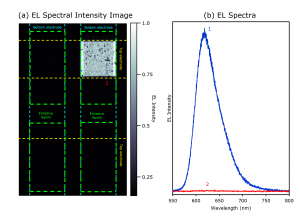
Figure 4. (a) Spectral EL image of OLED device. (b) EL spectra from points 1 and 2 labelled in the image in (a).
The EL intensity is not uniform across the active pixel, which has implications for the quality of the device. There are two vertical strips at the outer edges (white) of the emitting pixel that produces more EL than the rest of the pixel. Furthermore, there are many non-emissive regions in the pixel where the EL intensity is reduced. This indicates defects in the pixel as ideally, an OLED would exhibit intense and uniform emissions across each pixel.
High-Resolution Photoluminescence and Electroluminescence Spectral Imaging
To further investigate the effects seen in the PL and EL maps in the previous section, a smaller region on the EL active pixel, Figure 5a and b, was imaged using PL and EL. The upper region within the mapping grid was where the emissive layer overlapped with the electrodes, and the lower region was the emissive layer alone… The PL intensity image, Figure 5c, again shows that the top electrode attenuates the incoming laser and outgoing PL light, because the intensity from the electrode covered emissive layer is less than the uncovered emissive layer. The PL peak wavelength image, Figure 5d, shows that within the EL active electrode covered emissive layer, the PL emission is red-shifted (620 nm) compared to the uncovered emissive layer region (611 nm). This change in peak wavelength indicates that different energy levels are being accessed in the different regions.
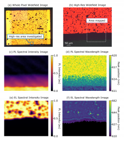
Figure 5. (a) Whole-pixel and (b) high-resolution widefield images of electroluminescent OLED pixel. (c) PL intensity and (d) peak wavelength images of the EL boundary of the OLED pixel. (e) EL intensity and (f) peak wavelength images of the same area.
The EL imaging shows that the less emissive defects in the pixel, Figure 5e, have a large redshift, Figure 4f, compared to the rest of the pixel. This is caused by the decrease in intensity of the EL band seen across the rest of the pixel, and the simultaneous increase in a second, lower energy EL band at 662 nm. Additionally, in the region at the very bottom of the EL active region in Figure 3, a blue shift occurs, which is consistent with the wavelength change seen across the PL image. All of these observations from high-resolution spectral imaging reveal a much greater level of complexity than would be detected with bulk PL and EL measurements of the complete OLED device.
High-Resolution Time-Resolved Photoluminescence and Electroluminescence Imaging
To obtain additional information TRPL and TREL imaging were performed on the same area, Figure 6. Here, the sample was subject to laser and electrical pulses for PL and EL, respectively and PL and EL lifetime decays of the OLED were recorded at 614 nm in MCS mode. The decays were fit with a single exponential decay model to extract the lifetime.
In the TRPL image in Figure 5a, the PL lifetime within the EL active region (upper region) was approximately 200 ns shorter than the PL lifetime in the EL inactive region (lower region). The longest and shortest lifetimes recorded were 800 ns and 600 ns, respectively, Figure 5b. A similar gradient was observed here to the PL intensity and wavelength images in Figure 4, where the emission became less intense going down the map and a blue shift occurred. Therefore, the TRPL data supports the conclusion that different energy levels are being accessed across the dopant strip when excited optically. In the TREL image in Figure 5b, the lifetime is similar across the entire region, approximately 470 ns. The EL lifetime was found to be significantly shorter than PL lifetime recorded within the same area.
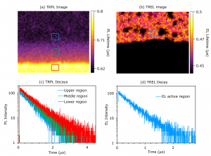
Figure 6. (a) Time-resolved PL image of OLED pixel. (b) Time-resolved EL image of OLED pixel. (c) PL lifetime decays from the image in (a). (d) EL lifetime decay from the image in (b).
Conclusion
In this Application Note, the RMS1000 Confocal Raman Microscope was used to perform PL, EL, TRPL, and TREL imaging of an OLED device. Combined, these various imaging modes provided detailed information about the location of the emissive layer and electrodes throughout the device; the efficiency and colour uniformity of a pixel within the device under working conditions; and relative information about the energy levels being accessed by the two processes.
Acknowledgements
We would like to thank the Organic Semiconductor Optoelectronics group at the University of St Andrews for providing the OLED used in this Application Note.
References
- A. Salehi et al., Recent Advances in OLED Optical Design, Adv. Funct. Mater., 2019, 29, 1808803, DOI: 10.1002/adfm.201808803.
- J. M. Ha et al., Recent Advances in Organic Luminescent Materials with Narrowband Emission, NPG Asia Mater., 2021, 13, 1–36, DOI: 10.1038/s41427-021-00318-8.
- T. Deksnys et al., Synthesis and Characterisation of a Carbazole-Based Bipolar Exciplex-Forming Compound for Efficient and Color-Tunable OLEDs, New J. Chem., 2017, 41, 559–568, DOI: 10.1039/C6NJ02865A.
