


Imaging Charge Extraction in VACNT Perovskite Solar Cells using Spectral and Lifetime Confocal Photoluminescence Mapping
Introduction
Halide perovskite solar cells are the subject of intense research interest due to the attractive properties of perovskite; high carrier mobilities, large absorption coefficients, tuneable bandgaps, and long carrier diffusion lengths. One of the challenges in any solar cell design is how to get the charge carriers efficiently out of the device. To aid charge extraction, electron and hole extraction layers are routinely incorporated into the device stack.
One promising material being investigated as a hole extraction layer are vertically aligned carbon nanotubes (VACNTs). A solar cell stack incorporating VACNTs as the hole extraction layer is shown in Figure 1. The VACNT isd grown in a grid pattern of ‘towers’ atop the ITO electrode in order to achieve improved charge extraction while maintaining high optical transmission through the ITO/VACNT.
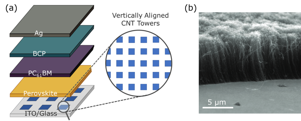 Figure 1: (a) Structure of a solar cell device stack utilising a VACNT as a hole extraction layer and (b) SEM image of the VACNT grown on the ITO substrate. Images adapted from Ferguson et al.1
Photoluminescence (PL) is proportional to the number of charge carriers in the perovskite and therefore sensitive to charge transfer into adjacent layers. This makes PL based techniques invaluable for investigating the performance of new extraction layers. In this application note, the hole transfer into a VACNT based hole extraction layer is imaged using steady-state and time-resolved confocal PL microscopy with an Edinburgh Instruments RMS1000 Confocal Raman & PL Microscope.
Experimental Setup
An array of VACNT towers were grown on an ITO coated glass substrate using photo-thermal chemical vapour deposition (PTCVD) and a layer of mixed halide Cs0.05FA0.79MA0.16PbI2.4Br0.6 perovskite was spin-coated on top. Full details of the sample fabrication can be found in a previous publication.1 The substrate was mounted onto a microscope slide using double-sided tape which was then secured to the motorised stage of the RMS1000 Confocal Raman & PL Microscope. The RMS1000 was equipped with a 532 nm CW laser for spectral acquisition, an EPL-450 picosecond pulsed diode laser for time-resolved, 600 gr/mm diffraction grating, back-illuminated CCD camera, time-correlated single photon counting (TCSPC) lifetime electronics, and a High-Speed PMT lifetime detector.
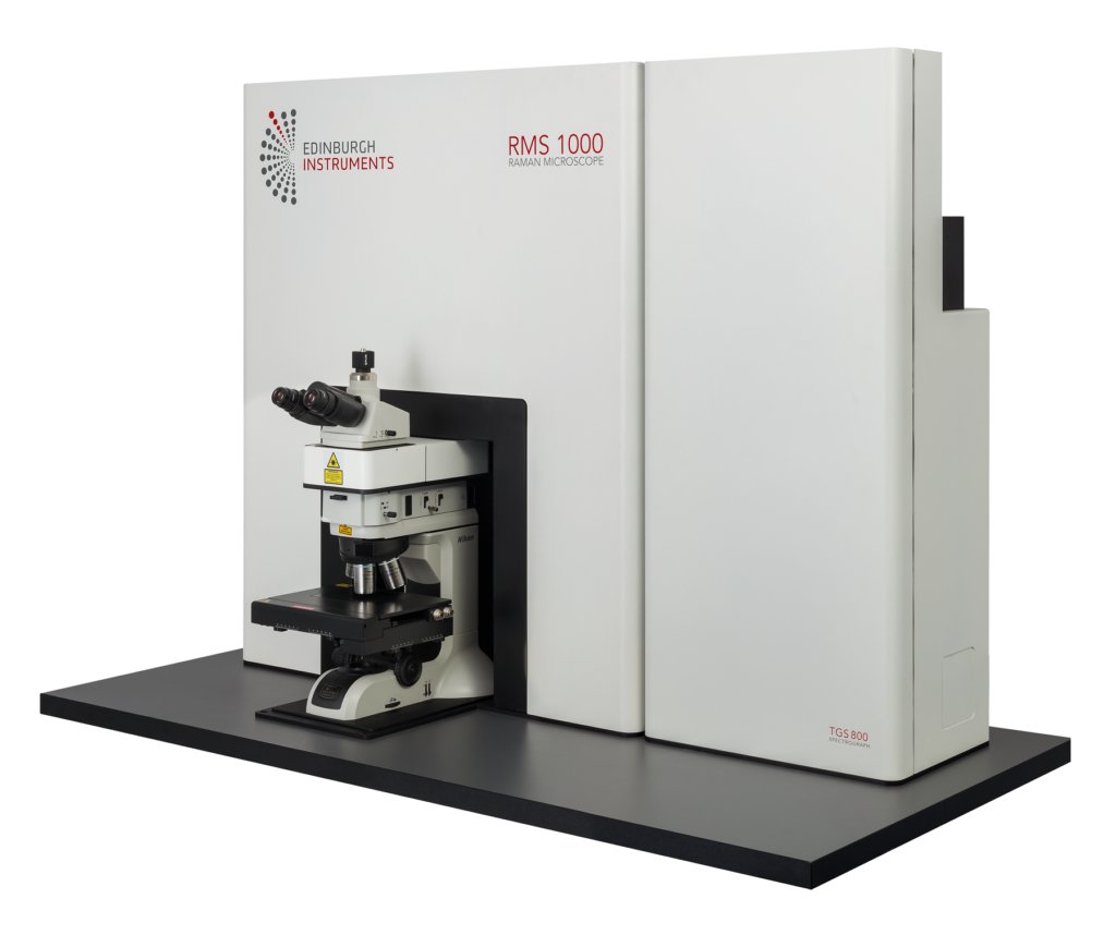 Figure 2: RMS1000 Confocal Raman & PL Microscope.
Spectral Photoluminescence Mapping
To observe hole transfer from the perovskite into the VACNT towers, the surface of the ITO/VACNT/Perovskite sample was imaged using PL intensity mapping. A reflected darkfield image of the 500 μm x 500 μm area to be mapped is shown in Figure 3a. The array of VACNT towers can be seen beneath the perovskite layer. A 100×100 point (5 μm resolution) PL map was acquired using a 532 nm laser for photoexcitation and recording the PL spectrum at each point using a 600 gr/mm diffraction grating and the CCD camera of the RMS1000. The integrated intensity of each PL spectrum was calculated to create the PL intensity map shown in Figure 3b.
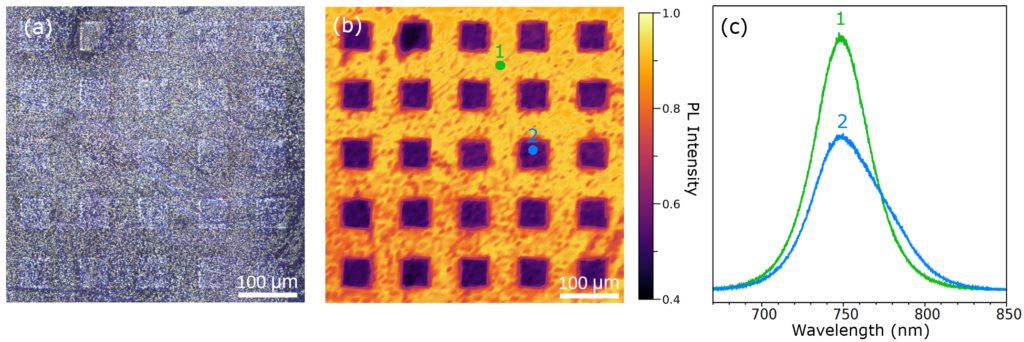 Figure 3: The ITO/VACANT/perovskite surface imaged using (a) widefield darkfield illumination, (b) confocal PL intensity mapping. Extracted spectra at points 1 and 2 of the PL map are shown (c).
The PL map shows that the PL intensity is reduced atop the VACNT towers which is indicative of hole transfer from the perovskite into the VACNTs. For PL to occur, the photogenerated electrons and holes in the perovskite must recombine. Hole transfer into the VACNTs will inhibit electron-hole recombination within the perovskite layer and lower the PL. The extracted PL spectra from an area with and without VACNTs present are shown in Figure 3c where a reduction in intensity and change in spectral shape can be seen.
Lifetime Photoluminescence Mapping
The PL intensity map provided strong evidence of hole transfer into the VACNT towers, however, it is not the only potential reason for reduced PL intensity. A thinner perovskite layer being deposited on top of the VACNTs would show a similar response for example. The RMS1000 can be equipped with pulsed laser sources and time-correlated single-photon counting (TCSPC) electronics for PL lifetime mapping. This provides complementary information to the spectral PL mapping, and be used as a confirmation measurement that hole transfer is occurring.
To acquire the PL lifetime map the sample was photoexcited with a 450 nm pulsed diode laser (EPL-450) and the PL lifetime measured using TCSPC with the High-Speed PMT lifetime detector of the RMS1000. 60 x 60 PL decays were acquired over a 150 μm x 150 μm area of the sample to give a 2.5 µm resolution lifetime map. The PL decays were fit with a three-component exponential model (Eq. 1) using the Ramacle® software of the RMS1000 and the intensity weighted average lifetime (Eq. 2) of the components calculated to create the lifetime map shown in Figure 4a.
 The PL lifetime map shows that the average PL lifetime of the perovskite decreases from ~100 ns to ~60 ns when VACNTs are beneath the perovskite. Example PL decays at positions with and without VACNTs present are shown in Figure 4b, highlighting the multi-exponential nature of the fitting required. The reduction in average lifetime atop the VACNT towers provides supporting evidence, that hole transfer into VACNTs is indeed occurring since hole transfer is an additional fast depopulation pathway that will shorten the PL lifetime.
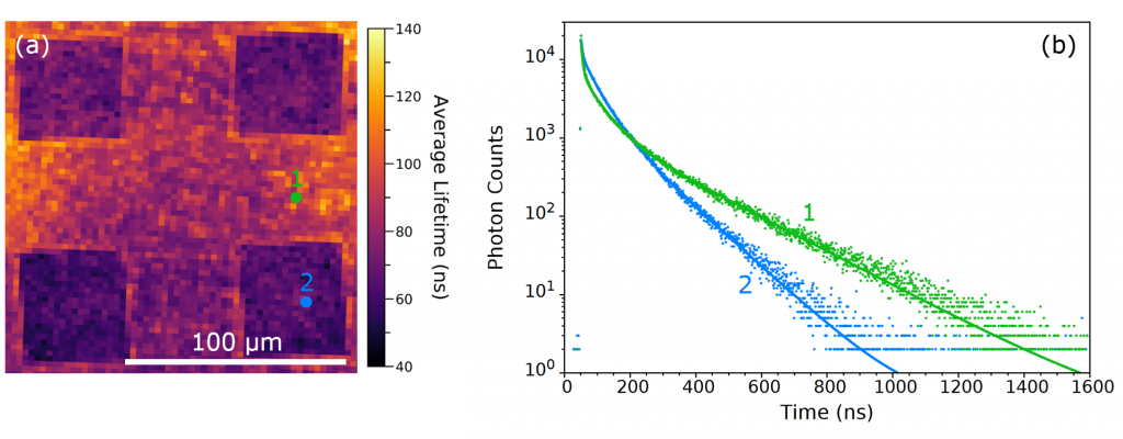 Figure 4: PL lifetime mapping of the perovskite sample. (a) Average PL lifetime map of the perovskite surface and (b) extracted PL decays (dots) and three-component exponential fits (solid lines).
Conclusion
The charge extraction properties of a VACNT hole extraction layer for perovskite solar cells were investigated using an RMS1000 Confocal Raman & PL Microscope. The RMS1000 can acquire both spectral and lifetime maps of semiconductor samples and the hole transfer into the VACNTs was confirmed using a combination of both PL mapping modes. Confocal PL microscopy is an ideal tool for visualizing charge extraction on the microscale in perovskite solar cells for the continued optimisation of cell performance.
Acknowledgements
We are grateful to Dr. Victoria Ferguson from the University of Surrey Nanoelectronics group for providing the perovskite sample used in this application note.
References
Discover the RMS1000 Confocal Raman & PL Microscope
Find out more about the RMS1000 Raman Microscope. If your work involves polymer phase transition and you would like to talk to one of our sales team to find out how the RMS1000 can be used within your own Raman research, please contact us. We’d be delighted to help.
Keep in Touch
If you have enjoyed reading this application note, why not sign-up to our monthly eNewsletter via the button below or follow us on your favourite social media channel in the footer below to keep up to date with our latest news and research.
