Cadmium telluride (CdTe) is a group II-VI compound semiconductor that is a promising active-light absorbing material for high-efficiency solar cells, Figure 1. It has the following advantages for solar technology:
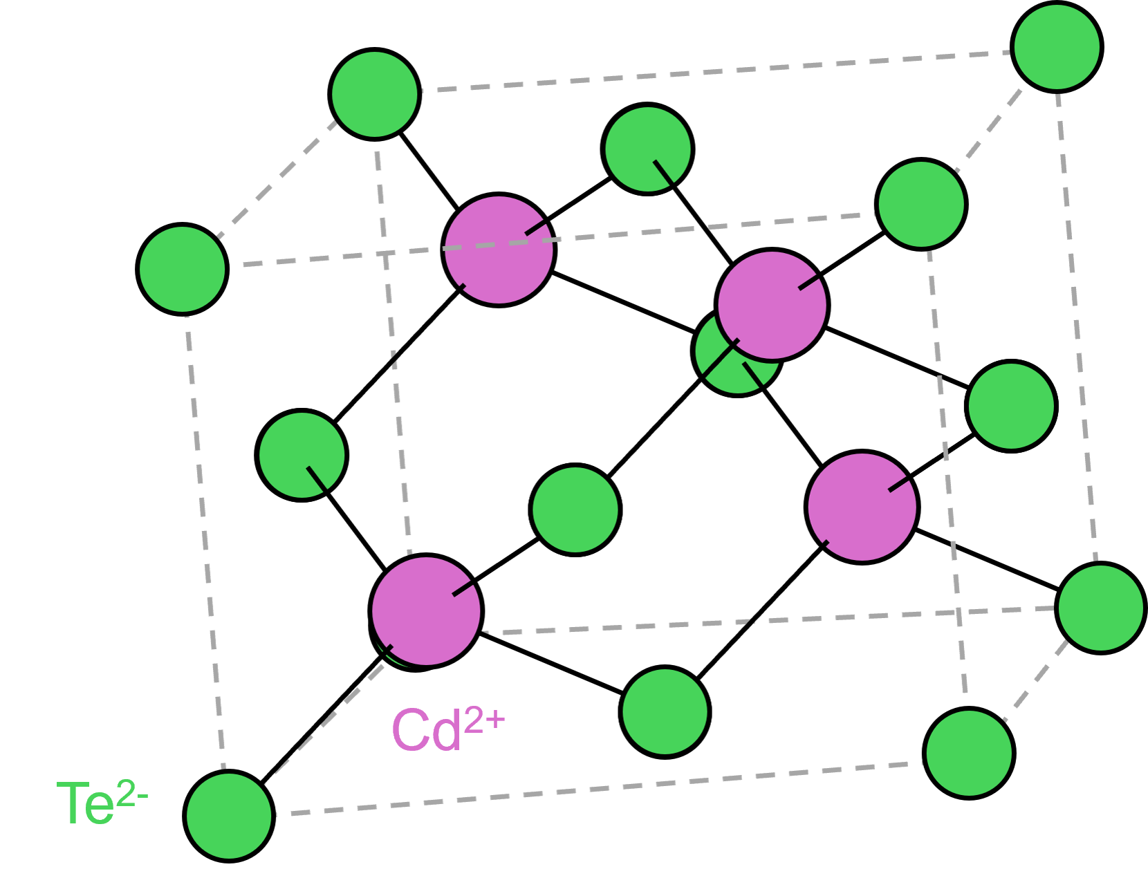
Figure 1. The crystal structure of cadmium telluride, CdTe. The pink spheres represent cadmium cations, Cd2+, and the green spheres represent telluride anions, Te2-.
To achieve high efficiency and consistently performing solar cells (and other optoelectronic devices), the semiconductor material must exhibit excellent and homogeneous crystalline quality. However, when the semiconductor material is deposited within the device as a thin film, as is the case with CdTe, surface irregularities can be introduced, which can lower cell efficiency.
Changes in the surface morphology of CdTe solar cells can impact performance in several ways:
As such, it is crucial to have techniques that can analyse surface roughness in CdTe thin-film solar cells, and its effect on the electronic and vibrational structure of the absorbing layer.
This Research Highlight showcases how the Edinburgh Instruments RM5 Confocal Raman Microscope, with integrated photoluminescence (PL) and Raman capabilities, was used by researchers at Universidad de Guadalajara for investigating the nanoscale surface roughness of CdTe wafers. This integrated approach allowed for a comprehensive understanding of the material’s properties.4
The sample was an undoped CdTe wafer with a (001) orientation and a cubic zincblende crystalline structure, shown in Figure 1. One side of the wafer was polished, and the other side was unpolished. Analysis was performed on the unpolished side as atomic force microscopy (AFM) had shown it exhibited nanoscale roughness.
The RM5, shown in Figure 2, facilitates both PL and Raman measurements sequentially. For PL characterisation, a 532 nm (2.3 eV) laser was used, with power control at 2.5 mW achieved through an integrated software-controllable neutral density filter. A 1200 gr/mm diffraction grating was used to enhance spectral resolution. Raman analysis was performed using a 785 nm (1.57 eV) laser, delivered to the sample at a power of 1 mW, and the same grating. The lasers required for PL and Raman were both internal to the system and were interchanged automatically in Ramacle® software.
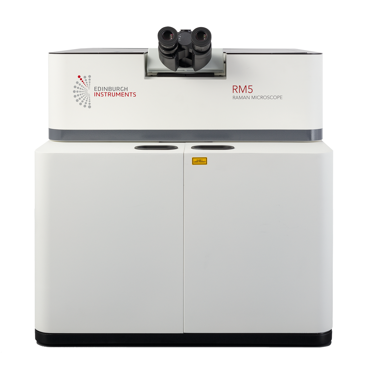
Figure 2. An image of the Edinburgh Instruments RM5 Confocal Raman Microscope.
Different regions on the CdTe wafer were found to exhibit different levels of surface roughness using AFM. PL spectra were obtained from three regions that exhibited surface roughness values of 307 nm (green), 467 nm (blue), and 602 nm (red), Figure 3.
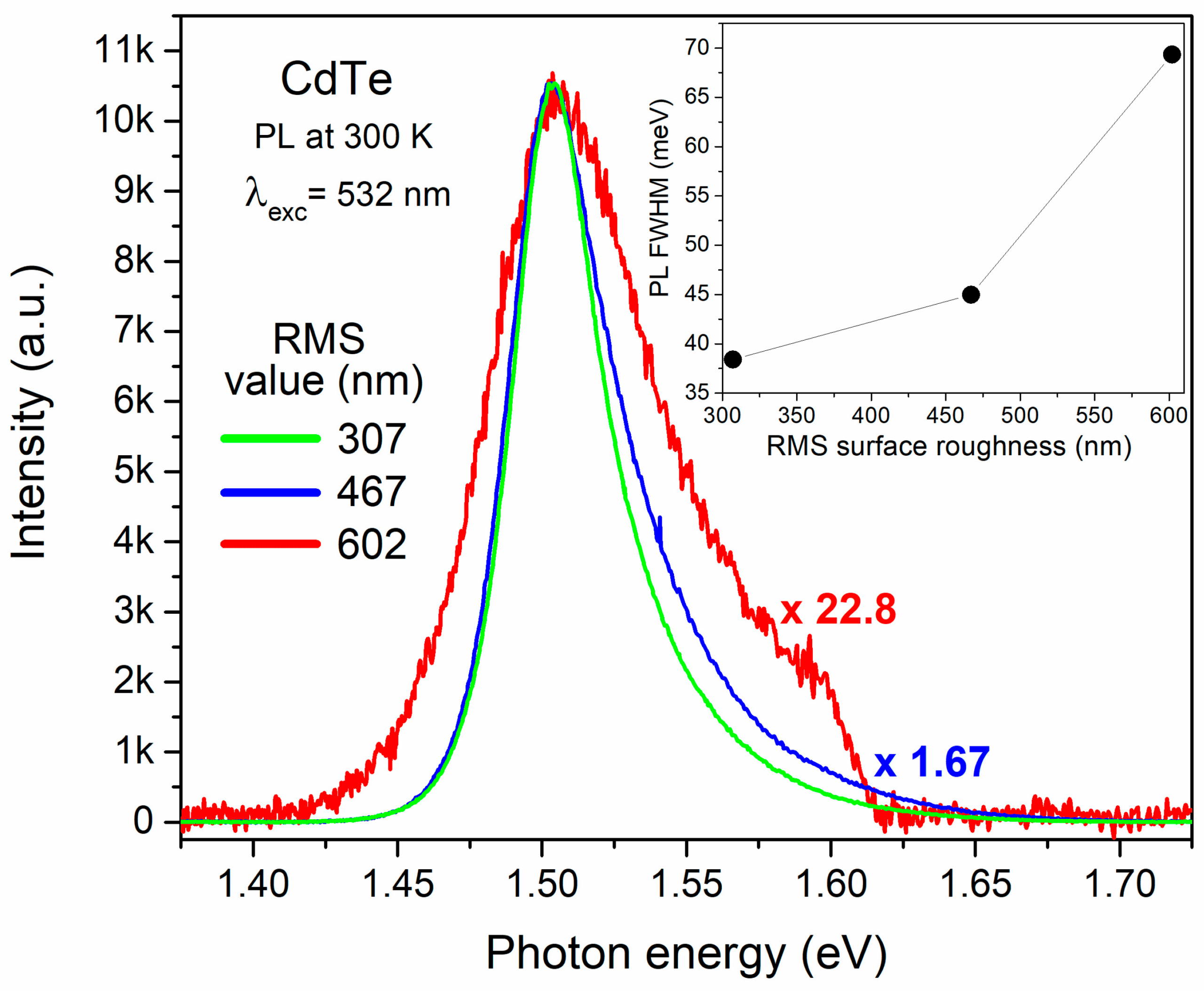
Figure 3. PL spectra of regions on a CdTe wafer with different surface roughness values. The inset shows the relationship between the full width at half maximum (FWHM) of the PL band and the value of roughness. The image is reprinted from Medel-Ruiz et al.4, Copyright (2024), with permission from MDPI through an Open Access Creative Common CC BY license.
The intensity and width of the PL response varied considerably across different regions of surface roughness on the CdTe wafer. The intensity of the 1.5 eV PL peak decreased with increasing surface roughness. Normalised PL data in Figure 3 shows that the PL intensity from the 307 nm roughness value region was 1.67 and 22.8 times greater than the 467 nm and 602 nm regions, respectively. This was attributed to the increase in scattering events by the uneven surface of the film, which reduces the probability of PL emission.
It was also observed that increasing the surface roughness led to a broader PL emission spectrum. The inset plot in Figure 3 shows that the FWHM of the PL peak was 38.42 meV, 44.98 meV, and 69.35 meV in the 307 nm, 467 nm, and 602 nm roughness value regions, respectively. The width of the PL spectrum of CdTe is explained not only by the bandgap, but also by the presence of various defect-related energy levels. These include native point defects, extended defects, and impurities. These defects create recombination and trapping centres (surface states) that affect carrier dynamics and recombination pathways.
As a result, a broadened PL emission spectrum can indicate the presence and interaction of various defect-related energy levels.This observation, clearly revealed by the sensitive detection capabilities of the RM5, directly correlates with decreased radiative recombination efficiency, a critical factor impacting overall solar cell performance.
Resonance Raman spectra were obtained from multiple regions on the wafer, which were found using AFM to have differing levels of nanoscale roughness, Figure 4. Resonance was achieved because the 785 nm laser used coincided with the bandgap of the material.
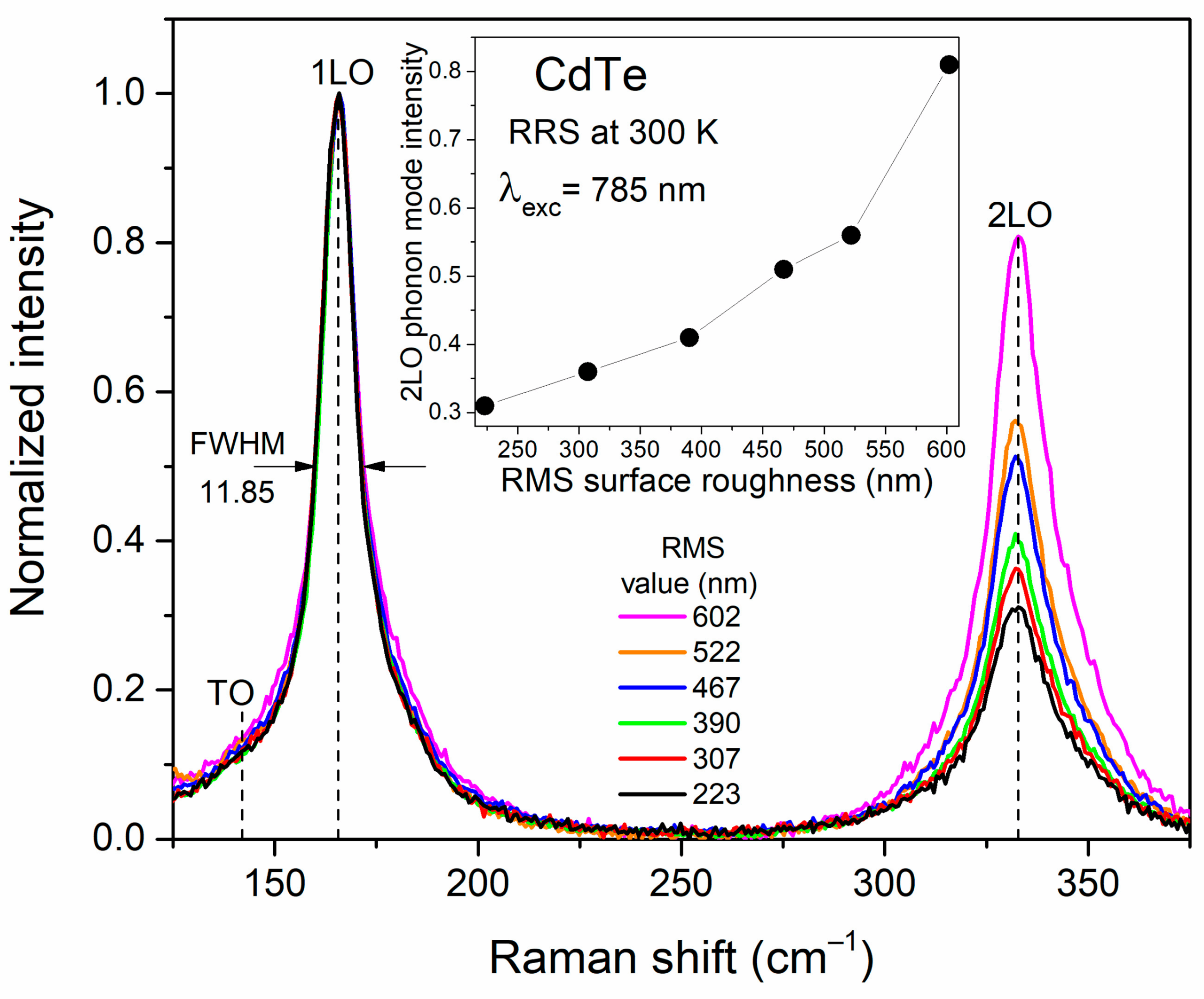
Figure 4. Resonance Raman spectra of regions on a CdTe wafer with different surface roughness values. The inset shows the relationship between the intensity of the 2LO band, relative to the 1LO, and the value of roughness. The image is reprinted from Medel-Ruiz et al.4, Copyright (2024), with permission from MDPI through an Open Access Creative Common CC BY license.
The spectra are shown between 125 and 375 cm-1 and are normalised to the first-order optical phonon (1LO) at 165.7 cm-1. Also observed in the spectra was an overtone band (2LO) located at 332.5 cm-1, which increased in intensity relative to the 1LO as the surface roughness increased. This observation was explained by the larger Raman shift of the 2LO band versus the 1LO band, which corresponds to a shorter wavelength. A phonon with a shorter wavelength oscillates over a shorter distance and is more sensitive to small-scale imperfections such as defects or surface irregularities. Surface roughness and defects, therefore, enable additional scattering pathways for 2LO phonons.
This enhances their Raman cross-section by increasing the phonon-light interaction time and allowing normally restricted scattering events, resulting in an overall increase in 2LO intensity.4 Their detection, therefore, can help gain insight into device functionality. Resonant excitation conditions further amplify this effect because the phonons also interact with electronic states.
The increase in the 2LO phonon mode can also be explained by the presence of additional modes under resonant conditions, which undergo phonon-phonon coupling with the 2LO phonon. Figure 5 shows the 1LO and 2LO peaks in resonant Raman scattering. Open circles represent an average of the experimental data from Figure 4, with the 2LO intensity normalised to 1LO. The main peaks (blue lines) were fitted using Lorentzian functions at 165.7 cm⁻¹ (1LO) and 332.5 cm⁻¹ (2LO).
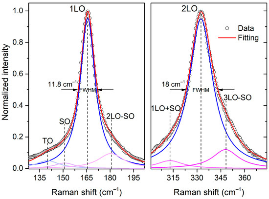
Figure 5. Lorentzian fitting the elementary contributions of the CdTe Raman spectra. The image is reprinted from Medel-Ruiz et al.4, Copyright (2024), with permission from MDPI through an Open Access Creative Common CC BY License.
A small peak at 151 cm⁻¹, attributed to the surface optical (SO) phonon mode, appears at the base of 1LO. This mode, which arises from surface vibrations, is usually weak but is amplified under resonance conditions. The TO (141 cm⁻¹) and SO (151 cm⁻¹) modes were identified and fitted. The TO mode, normally forbidden in bulk CdTe (001), becomes Raman-active due to surface symmetry breaking.
A high-frequency shoulder on the 1LO peak suggests 2LO–SO phonon coupling. The broadening of the 2LO base is due to multi-phonon coupling between the SO mode and 1LO phonon. Peaks at 313 cm⁻¹ (1LO+SO) and 348 cm⁻¹ (3LO−SO) confirm these interactions.5,6 When the energy of phonon-phonon interactions coincides with the 2LO phonon energy, resonance occurs, enhancing the Raman intensity of the 2LO peak by increasing scattering probability. These additional modes contribute to the broadening and strengthening of the 2LO peak by increasing the number of scattering events that can produce phonons. Under resonant Raman conditions, this effect is further amplified, as phonon-phonon interactions become more efficient due to enhanced electron-phonon coupling.
Understanding these phonon fingerprints under resonant conditions offers a powerful, non-destructive route to characterising surface quality, a crucial factor dictating the ultimate performance and reliability of CdTe-based devices.
Understanding surface roughness in CdTe thin films is crucial for improving the efficiency and longevity of next-generation solar cells. This study highlights how PL and resonance Raman microscopy with the RM5 can serve as powerful, non-destructive tools for probing nanoscale surface variations in CdTe wafers. The findings reveal that increased surface roughness is correlated with lower PL intensity, broader emission spectra, and enhanced 2LO phonon activity in Raman spectra, simultaneously highlighting the impact of structural irregularities on both electronic and vibrational properties. These findings underscore the critical role of advanced spectroscopic tools, such as the RM5, in providing the detailed material characterisation needed to optimise next-generation solar cell technologies.
This Research Highlight is based on an article published in Applied Sciences. The full article can be found here: https://www.mdpi.com/2076-3417/14/17/7680.