Skip to content
Skip to content
  • News
  • Events
  • eBooks
  • Blog
  • Careers
  • Contact
  • News
  • Events
  • eBooks
  • Blog
  • Careers
  • Contact
KNOWLEDGEBASE
  • About Us
  • Products

    Fluorescence Spectrometers

    • FLS1000 Photoluminescence Spectrometer
    • FS5 Spectrofluorometer
    • LifeSpec II Lifetime Spectrometer
    • Mini-tau Lifetime Spectrometer

    Raman Microscopes

    • RM5 Raman Microscope
    • RMS1000 Multimodal Confocal Microscope

    Transient Absorption

    • LP980 Transient Absorption Spectrometer

    FTIR Spectrometers

    • IR5 FTIR Spectrometer

    Lasers and LEDs

    • Pulsed Lasers
    • Gas Lasers
    • Customisation Options
    View All Products
  • Techniques
  • Applications
KNOWLEDGEBASE
Edit Content
  • About Us
  • Products
  • Techniques
  • Applications
  • Knowledgebase
  • eBooks
  • News
  • Events
  • Blog
  • Careers
  • Contact Us
  1. Home
  2. Blog Post
  3. Map of the Month – Mapping Defects in Perovskite Solar Cells

BLOG

Map of the Month – Mapping Defects in Perovskite Solar Cells

  • May 1, 2023
Edit Content

Welcome to Edinburgh Instruments’ monthly blog celebrating our work in Raman, Photoluminescence, and Fluorescence Lifetime Imaging. Every month we will highlight our pick for Map of the Month to show how our spectrometers can be used to reveal all the hidden secrets in your samples.

May

With much of the world aiming to become completely independent of fossil fuels in the near future, there is an urgent need for alternative energy sources that produce less greenhouse gas and pollutant emissions, lower the future risk of climate change, and help to mitigate economic and energy security concerns surrounding the volatility of oil and gas prices in response to geopolitical events. Solar power is an alternative energy source that converts energy from the sun into electricity. It is highly desirable because, unlike fossil fuels, the sun’s energy is infinite, and the technology is emission-free.

Photovoltaic cells found within solar panels rely on semiconductor materials that absorb sunlight and generate electrons that flow into conducting electrodes to produce current, Figure 1.  The primary semiconductor material used in solar cells is silicon, which has the advantage of being abundant and stable, as well as having optical properties that align well with solar radiation. The disadvantage of using silicon is that the large crystals used require an expensive and complex manufacturing process that is energy intensive. Perovskites have emerged as a promising alternative to silicon because of their relatively simple and cheap additive deposition manufacturing techniques and compositional flexibility which affords a high degree of optical tunability. Improvements in perovskite photovoltaic cell efficiencies have been rapid and dramatic since they were first developed, and they are now competitive with crystalline silicon cells in that regard. However, it is also the case that perovskites are prone to suffer from defects that affect cell crystallinity, energy band alignment, and non-radiative charge recombination, all of which can reduce device performance.

Figure 1. A perovskite photovoltaic cell.

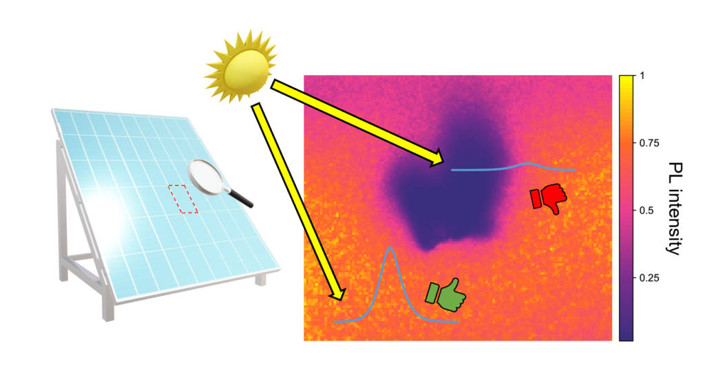
In this instalment of Map of the Month, we used the RMS1000 Raman Microscope to image the steady-state photoluminescence response, characteristic of band-to-band recombination, of a segment of a mixed halide perovskite thin film containing a suspected large defect, shown in Figure 2.

Figure 2. Stitched brightfield image of a perovskite thin film containing a suspected defect.

The red square around the defect in the brightfield image in Figure 2 is the area that was designated for imaging, and the resulting photoluminescence intensity map is shown in Figure 3A. It can be seen in this map that the photoluminescence emitted from the area corresponding to the suspected defect is significantly reduced in comparison to the surrounding film, which in a complete solar cell would translate to reduced power conversion. The corresponding spectra from high and low-intensity regions on the map, Figure 3B, show that the photoluminescence wavelength also shifts across the map. The difference in peak wavelength between the spectra extracted from the surrounding film and the defect structure was 34 nm, which suggests the band gap and hence the morphology of the perovskite structure is different in the two regions.

Figure 3. Photoluminescence imaging of a perovskite thin film using the RMS1000 Raman Microscope.

RELATED PRODUCTS

RM5

Raman Microscope

VIEW

RESOURCES

Tags:
  • Map of the Month
  • Photovoltaics
  • RMS1000
  • Photoluminescence
  • Raman
Related Posts:

No results found.

Application Notes:
Featured Product:

RMS1000 Raman Microscope

View more »
Suggested Reading:

No results found.

Share:
PrevPrevious
NextNext

Keep up to date with the latest from Edinburgh Instruments

Join our mailing list and keep up with our latest videos, app notes and more!

LOCATION:
  • Edinburgh Instruments Ltd.
    2 Bain Square, Kirkton Campus, Livingston, EH54 7DQ.
  • sales@edinst.com
  • +44 1506 425 300
ABOUT:
  • About Us
  • Techniques
  • Applications
  • Knowledgebase
  • About Us
  • Techniques
  • Applications
  • Knowledgebase
PRODUCTS:
  • Fluorescence Spectrometers
  • Raman Microscopes
  • UV-Vis Spectrophotometers
  • Transient Absorption
  • FTIR Spectrometers
  • Lasers and LEDs
  • Customisation Options
  • Software
  • Upgrades
  • All Products
  • Fluorescence Spectrometers
  • Raman Microscopes
  • UV-Vis Spectrophotometers
  • Transient Absorption
  • FTIR Spectrometers
  • Lasers and LEDs
  • Customisation Options
  • Software
  • Upgrades
  • All Products
LEGALS:
  • News
  • Events
  • Blog
  • Careers
  • Contact Us
  • Terms and Conditions
  • Privacy Policy
  • News
  • Events
  • Blog
  • Careers
  • Contact Us
  • Terms and Conditions
  • Privacy Policy
SOCIALS:
Youtube Linkedin X-twitter Facebook
©2024 Edinburgh Instruments. Registered in England and Wales No: 962331. VAT No: GB 271 7379 37
Manage Consent
To provide the best experiences, we use technologies like cookies to store and/or access device information. Consenting to these technologies will allow us to process data such as browsing behaviour or unique IDs on this site. Not consenting or withdrawing consent, may adversely affect certain features and functions.
Functional Always active
The technical storage or access is strictly necessary for the legitimate purpose of enabling the use of a specific service explicitly requested by the subscriber or user, or for the sole purpose of carrying out the transmission of a communication over an electronic communications network.
Preferences
The technical storage or access is necessary for the legitimate purpose of storing preferences that are not requested by the subscriber or user.
Statistics
The technical storage or access that is used exclusively for statistical purposes. The technical storage or access that is used exclusively for anonymous statistical purposes. Without a subpoena, voluntary compliance on the part of your Internet Service Provider, or additional records from a third party, information stored or retrieved for this purpose alone cannot usually be used to identify you.
Marketing
The technical storage or access is required to create user profiles to send advertising, or to track the user on a website or across several websites for similar marketing purposes.
Manage options Manage services Manage {vendor_count} vendors Read more about these purposes
View preferences
{title} {title} {title}