As semiconductor devices get smaller and their power densities increase, understanding temperature effects at the micro- and nanoscale becomes increasingly important. Temperature-dependent (TD) Raman microscopy is a powerful and non-destructive method that can probe the thermal and electronic properties of semiconductor materials with sub-micron spatial resolution.
Higher temperatures influence crucial properties of semiconductors, leading to increased conductivity, reduced resistance, and shifts in the Fermi level.1 These properties are intimately linked to the performance of the final device. It is, therefore, essential to have sensitive and specific techniques for probing the properties of these materials at different temperatures.
In this Application Note, we demonstrate the power of TD Raman microscopy by investigating the temperature-induced Raman spectral changes in a silicon (Si) chip with an Edinburgh Instruments RM5 Confocal Raman Microscope equipped with a Linkam stage. We show that Raman microscopy can be used to track changes in the electrical properties of the material, such as Fano resonance and the Fermi level.
The sample analysed was a 10 mm x 10 mm chip from an n-doped Si wafer. The chip was placed in a Linkam THMS600 Heating and Cooling Stage, which allows for temperature control in a range between 78 K and 873 K.
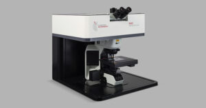
The stage was fixed underneath the microscope of an RM5 equipped with a 50X 0.5 NA long-working distance objective, a 532 nm laser and a 2400 gr/mm diffraction grating, Figure 1, which allowed for very high spectral resolution to be achieved. Spectral band widths were calculated using a twice-smoothed Lorentzian function in Ramacle® software. The temperature of the stage was controlled using Ramacle, and spectra were recorded between 173 K and 473 K in 25 K steps.

Figure 1. An n-doped Si wafer inside a Linkam THM600, fitted to an RM5
One of the most crucial properties of semiconductor materials is the Fermi level, EF. Understanding how it is affected by doping and temperature is important for tailoring the conductivity of a semiconductor in various electronic applications. In this section, we will cover how TD Raman spectra contain information about EF.
In band-structure theory, which describes the energy levels in a semiconductor, the EF is a statistical quantity representing the energy at which the probability of an electron occupying the valence or conduction band is 50%. The position of EF relative to the conduction band determines the material’s conductivity.
Figure 2 illustrates how the relationship between EF and temperature differs for intrinsic and extrinsic semiconductors. In a simple intrinsic semiconductor, one which has not been doped, the EF is very close to the halfway point between the two bands regardless of the temperature. This is because each electron promoted to the conduction band leaves a positive hole in the valence band.
In an n-doped extrinsic semiconductor, such as the Si chip used in this Application Note, the EF lies between the donor level and the conduction band at 0 K and gradually tends towards an intrinsic semiconductor’s EF as the temperature increases. This indicates that as donor electrons are depleted, intrinsic electrons begin to contribute more to the electrical conductivity of the material. The reverse is true for a p-doped extrinsic semiconductor, meaning that EF gradually increases from below the acceptor level with temperature.
 intrinsic, (B) n-doped, and (C) p-doped semiconductors.")
Figure 2. The relationship between the Fermi level, EF, and temperature in (A) intrinsic, (B) n-doped, and (C) p-doped semiconductors.
TD Raman microscopy can be used to probe EF in a semiconductor and its thermally induced shift in a relatively simple manner compared to traditional techniques such as X-ray or ultra-violet photoelectron spectroscopy. In both p- and n-doped Si, the asymmetrically broadened Raman spectral line width of the LO phonon mode contains information about the EF position through a phenomenon known as Fano resonance.2,3 This arises from the interference between discrete inter-band transitions and the electronic continuum.
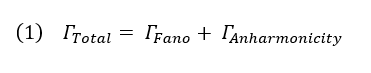
Asymmetric Fano broadening varies with temperature because of changes in the EF, which describes the position of the electronic continuum. Information about it is contained in the width of the LO phonon mode, ΓTotal (Equation 1), along with anharmonicity-induced broadening, which can be calculated using a Balkanski model.4
The spectra in Figure 3A show Raman spectra recorded on an n-doped Si chip between 173 K and 473 K in 25 K steps. These spectra show that as the temperature increases, the intensity of the dominant LO phonon band in Si (ca. 520.5 cm-1 at room temperature) decreases, and the position of the band gradually shifts to a lower wavenumber.
It is not immediately clear from the spectra alone that the width of the phonon mode is changing with temperature. However, when the spectra are normalised and converted to an image where the X-axis is Raman shift, the Y-axis is temperature, and the Z-axis is Raman intensity, Figure 3B, it can be observed that the phonon mode becomes gradually wider with increasing temperature.
 Raman spectra recorded from an n-doped Si chip between 173 K and 473 K in 25K steps. (B) Temperature map of the same spectra normalised.")
Figure 3. (A) Raman spectra recorded from an n-doped Si chip between 173 K and 473 K in 25K steps. (B) Temperature map of the same spectra normalised.
Figure 4 presents the variation in LO phonon mode width, measured via FWHM, for n-doped Si between 173 K and 473 K. At 173 K, the FWHM is 4.2 cm-1, while at 473K, it increases significantly to 6.2 cm-1. This increase in peak width in temperature has previously been assigned to increased Fano resonance over anharmonicity effects, and an increase in ΓFano is associated with a decrease in EF.3 More information about how EF can be calculated directly from the FWHM of the silicon LO phonon mode is available in Rani et al.3 Briefly, the EF can be calculated using only ΓFano, which can be determined using a Fano line fit and removing the effects of ΓAnharmonicity, which are calculated independently using the Balkanski model. An increase in ΓFano, is related to a decrease in EF.

Figure 4. A plot showing the LO phonon FWHM for an n-doped Si chip against temperature. The linear regression reveals a strong correlation between the two variables.
This data shows that as the temperature of the n-doped Si chip is increased, the FWHM of the LO phonon mode increases because the material gradually begins to behave like an intrinsic semiconductor, and EF decreases towards the midway point between the valence and conduction band.
In p-doped Si, the FWHM of the LO phonon decreases with temperature, which represents the EF increasing towards the midway point between the two bands. Like in the previous section, this data is only meaningful when the collection volume on the Si chip is free from other effects that would broaden the Raman spectrum, such as strain and crystallinity differences.
This is not only a promising method for characterising the electronic properties of silicon; it is valid for any material where Fano resonance occurs, such as molybdenum disulfide, graphene, and cadmium telluride.2,5,6
TD Raman microscopy is a powerful tool for probing the thermal and electronic properties of semiconductors. By monitoring the LO phonon mode in an n-doped Si chip from 173 K to 473 K, we demonstrated the ability of the technique to track key electronic properties like the Fermi level and Fano resonance.