Semiconductors are the linchpin of the modern electronics industry. When fabricating semiconductor devices, the number of defects in the constituent semiconductor materials must be tightly controlled. The presence of defects in the semiconductor can affect a device’s yield, performance, and reliability.1
Raman spectroscopy is an excellent technique for inspecting semiconductor materials because it is highly sensitive to even the most subtle changes in the optical properties of the crystal lattice.2 Defects cause distortions and strain in the surrounding crystal lattice, leading to altered optoelectronic properties that can be probed using Raman spectroscopy. Raman is extremely powerful when coupled with a microscope because it can image the variation in properties across the semiconductor. In this Application Note, an Edinburgh Instruments RM5 Raman microscope was used to analyse and image the strain from a defect in a silicon semiconductor wafer.
All measurements were performed on an RM5 using a 532 nm laser and a 2400 gr/mm diffraction grating. Silicon semiconductor wafers were purchased from PI-KEM. A defect was created on one of the wafers by making an indent on the material. The defect was imaged using SurfMAP® to ensure the sample remained in focus throughout the measurement. Peak position and peak width maps were created in Ramacle®.

Figure 1. RM5 Raman Microscope.
Crystalline silicon is the most common semiconductor material used in electronic devices. It produces a characteristic spectrum when probed using Raman spectroscopy, as shown in Figure 2.3 The dominant feature in the spectrum is a sharp peak at 521 cm-1, which is highly sensitive to structural and optoelectronic changes in the material.
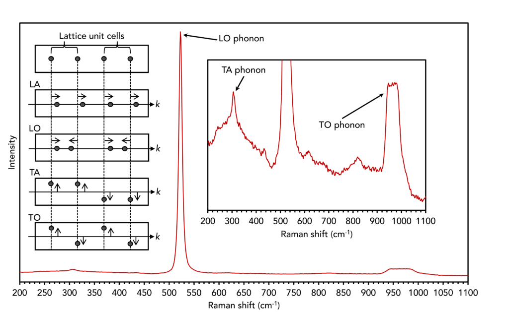
Figure 2. Raman spectrum of silicon with inset schematic illustrating phonon modes.
In crystalline lattice materials such as silicon, Raman modes occur through inelastic light scattering by phonons, which are quanta with energies proportional to lattice vibrations. Phonons are characterised by the phase in which atoms within a lattice unit cell oscillate and their oscillation direction with respect to a propagating wave, which is illustrated in the inset in Figure 2. When atoms in the unit cell oscillate in phase, the phonon is named acoustic, and when they oscillate out of phase, the phonon is named optical. Oscillations that are parallel or
perpendicular to the propagating wave are further named longitudinal and transverse, respectively. In the silicon Raman spectrum, the main peak at 521 cm-1 arises from a longitudinal optical (LO) phonon, and the weaker peaks at 305 cm-1 and 965 cm-1 are the transverse acoustic (TA) and transverse optical (TO) phonons, respectively.
Strain is common in solid-state materials and is defined as the change in the positions of atoms and inter-atom distances induced by stress, which is the force applied to the material. To investigate the effect of strain on the optical properties of silicon, a stress-induced defect was located on the wafer, observable in the widefield optical image in Figure 3a.
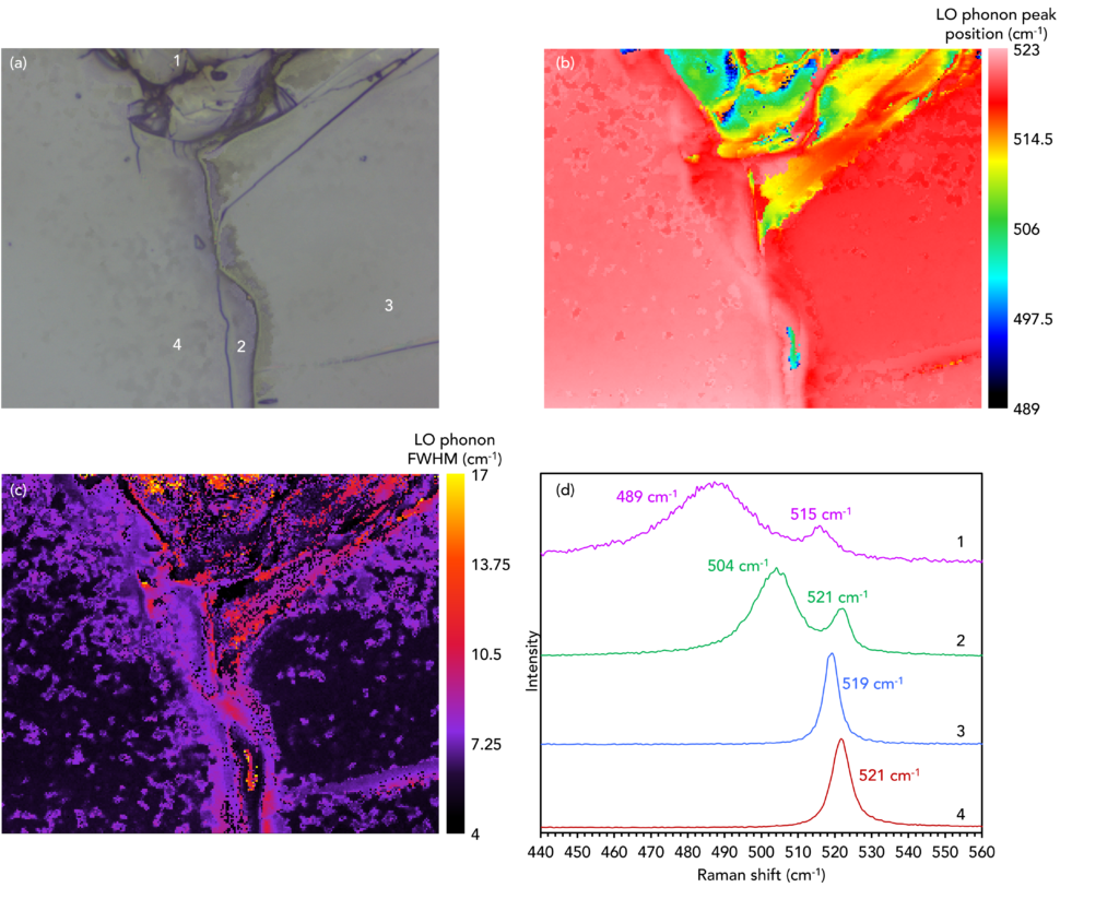
Figure 3. Raman mapping of a defect and the surrounding area on a silicon semiconductor wafer.
The defect and surrounding area were analysed using Raman imaging. Significant differences in the peak position (Figure 3b) and full-width half maximum (FWHM) (Figure 3c) of the LO phonon mode were observed, which is associated with changes in strain and crystallinity of the silicon. Raman spectra from various points on the maps are shown in Figure 3d and their locations are marked in Figure 3a.
In the peak position map, the LO phonon mode shifted between 521 cm-1 and 518 cm-1 on the regions surrounding the defect. This is consistent with tensile strain in the material; as the lattice structures elongate, the atoms become further apart, and vibrations decrease in energy relative to the unstrained material.4 Additionally, more significant peak shifts of up to 32 cm-1 were observed in the defect, which suggested the presence of nanocrystalline silicon.5
The FWHM map corroborates the presence of different crystallinity states within the wafer. The extreme broadening of the LO phonon (4 cm-1 to 17 cm-1) in the defect indicates phonon confinement associated with the presence of nanocrystalline silicon.6 The moderate phonon broadening in the region surrounding the defect is attributed to a distribution of unresolvable strain states.
Raman microscopy is an effective and sensitive technique for monitoring the optoelectronic properties of silicon semiconductors. Raman imaging of a silicon wafer defect revealed the presence of strain and different crystallinity states within the material.
1. S. Mahajan et al., Defects in semiconductors and their effects on devices, Acta Mater., 2000, 48, 137-149.
2. D. Yamashita et al., Raman shift and strain effect in high-Q photonic crystal silicon nanocavity, Opt. Express, 2015, 23, 3951-3959.
3. J. H. Parker et al., Raman Scattering by Silicon and Germanium, Phys. Rev., 1967, 155, 712-714.
4. F. Ureña et al., Raman measurements of uniaxial strain in silicon nanostructures, J. Appl. Phys., 2013, 114, 114507.
5. S. V. Gaisler et al., Analysis of Raman spectra of amorphous-nanocrystalline silicon films, Phys. Solid State, 2004, 46, 1528-1532.
6. V. Paillard et al., Improved one-phonon confinement model for an accurate size determination of silicon nanocrystals, J. Appl. Phys., 1999, 86, 1921-1924.