Silicon carbide (SiC) is a semiconductor regularly used in transistors for high-power electronic devices such as inverters in electric vehicles and solar panel grids.
SiC is considered a superior material to silicon for these applications because it has the following properties:
SiC therefore excels in applications where efficiency, size and thermal management of devices are important.
To ensure these advantages are fully realised, manufacturers must monitor and control crystal structure, crystal quality, dopant concentration, and defects in the SiC, which can all heavily influence the properties of the material.
In this Application Note, we use the Edinburgh Instruments RM5 to demonstrate that Raman microscopy is the ideal technique for identifying structural and electronic parameters in SiC rapidly, reproducibly, non-destructively, and without direct contact.
All measurements were performed on an RM5 using a 532 nm laser and an 1800gr/mm diffraction grating, Figure 1. These settings enable a high spectral resolution to be achieved, which is crucial for identifying spectral changes associated with the structure of the material. The sample analysed was a wafer of n-type, nitrogen-doped, 4H-SiC.
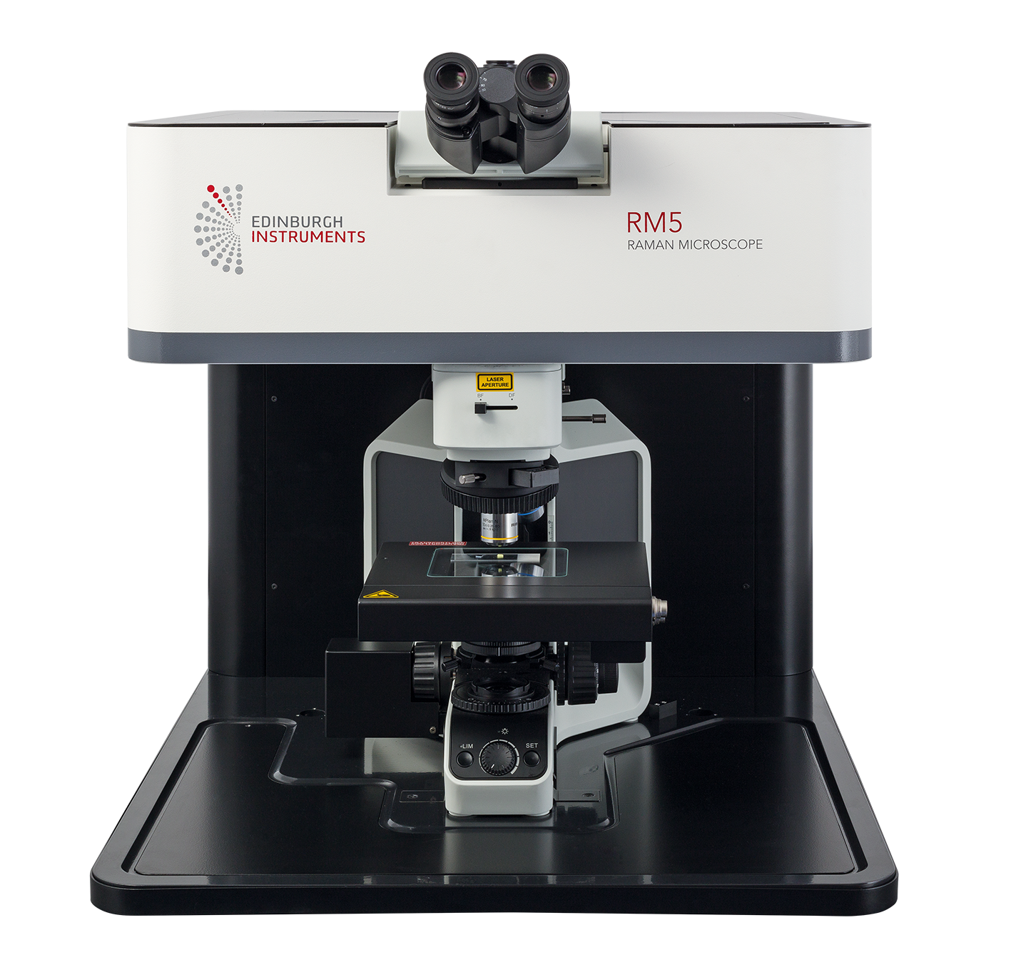
Figure 1. Edinburgh Instruments RM5 Confocal Raman Microscope.
The crystalline structure of a SiC wafer strongly impacts the physical and electronic properties of the material. SiC can exist in 250 known polytypes; each has the same chemical composition but different crystallographic structures with unique point groups and/or stacking sequences. The SiC tetrahedron and three of the most common polytypes, 3C-SiC, 4H-SiC, and 6H-SiC, are illustrated in Figure 2.
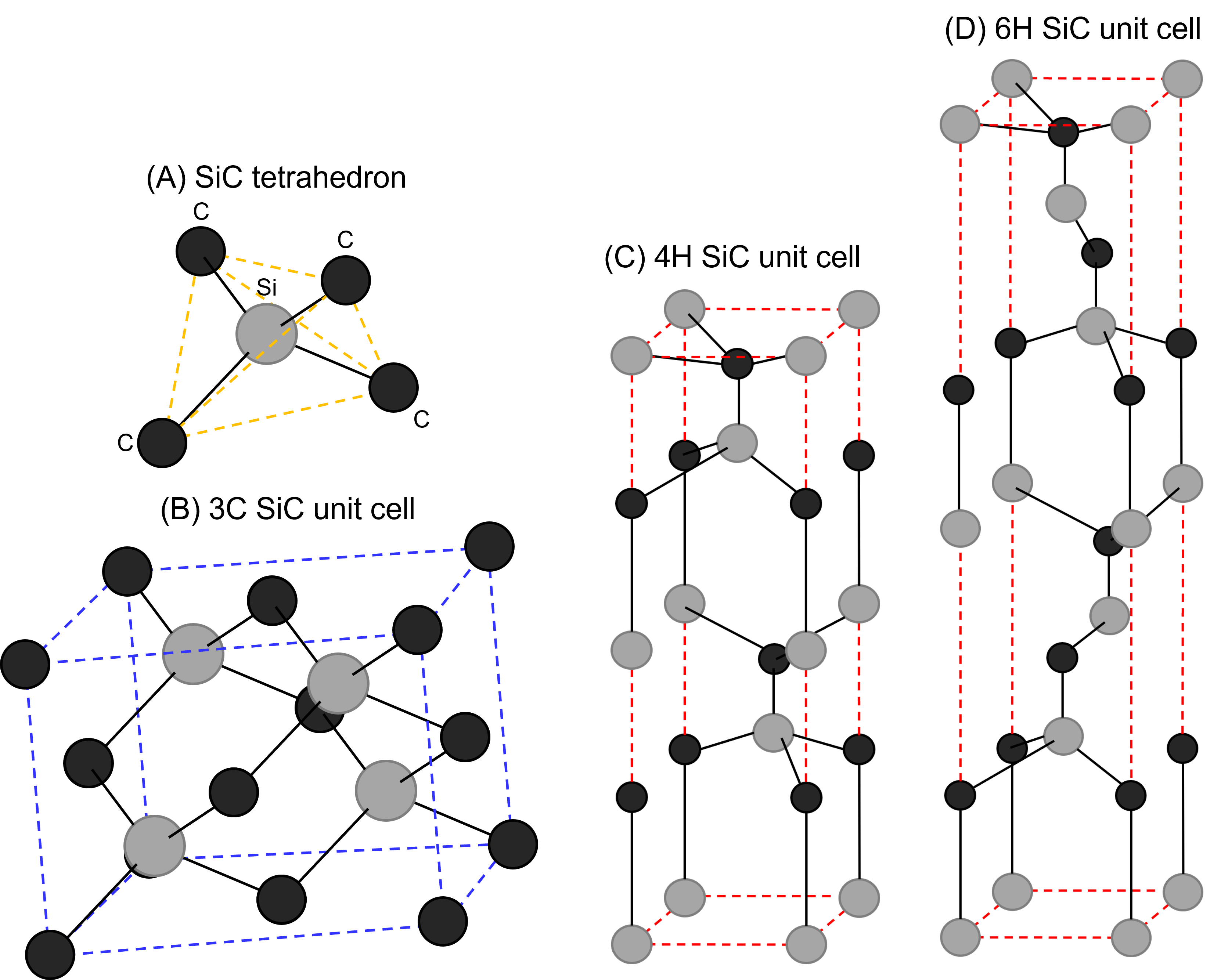
Figure 2. Schematics of the (A) SiC tetrahedron, (B) 3C-SiC unit cell, (C) 4H-SiC unit cell, and (D) 6H-SiC unit cell. Schematics (B) – (D) represent three of the 250 known polytypes of SiC.
In this naming convention, the letter represents the crystallographic point group, and the number represents the number of atomic layers in the unit cell. For example, ‘C’ and ‘H’ represent cubic and hexagonal symmetry, respectively. 4H-SiC and 6H-SiC have hexagonal symmetry, but they differ because 4H-SiC has four layers in the unit cell, whereas 6H-SiC has six. These different polytypes have different bandgaps and charge carrier mobilities, which is why it is crucial to be able to differentiate between them.
The Raman spectrum of 4H-SiC was analysed and is shown in Figure 3. 4H-SiC belongs to the C6v point group, which has Raman active modes with A1, E1, and E2 symmetry. In the Raman spectrum, the most dominant bands are labelled: the band at 205 cm-1 is an E2 transverse acoustic (TA) phonon mode, 610 cm-1 is A1 longitudinal acoustic (LA), 777.0 cm-1 is E2 transverse optical (TO), and 983.0 cm-1 is A1 longitudinal optical (LO).1 An explanation of phonon modes is provided in our Application Note on silicon semiconductors.
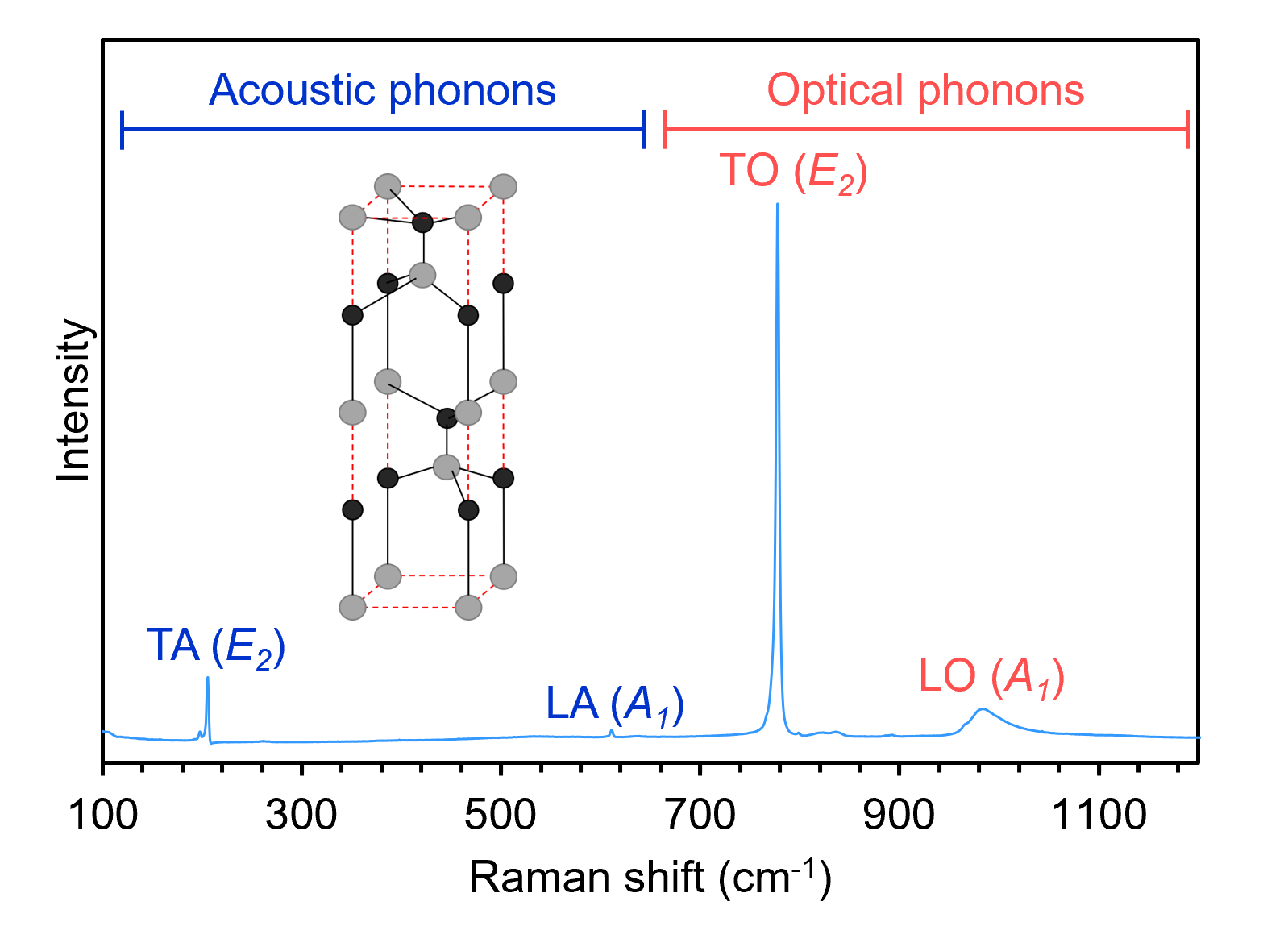
Figure 3. Raman spectrum of a 4H-SiC wafer with acoustic and optical phonon modes labelled.
The Raman spectra of 3C-SiC and 6H-SiC differ subtly from 4H-SiC. In 3C-SiC, which belongs to the Td point group, the TO band is at a higher Raman shift than 4H-SiC, as is the LO band. Also, the ratio between the TO and LO bands is much closer to one, and there are no TA and LA bands in 3C-SiC.2
6H-SiC also belongs to the C6v point group, but the spectrum differs from 4H-SiC because of the different stacking arrangements. In 6H-SiC, the TA and LA modes both occur at higher Raman shifts and the TO E2 band is diminished in proportion to a dominant TO E1 band at 797 cm-1.2 We will see an example of this in a later section when we analyse defects.
Since each polymorph exhibits a unique Raman spectrum, the technique can readily be used to characterise the crystal structure in SiC wafers and devices and optimise electronic and physical performance.
Doping a semiconductor is an essential process in the development of diodes and transistors. Devices such as metal-semiconductor field-effect transistors (MESFETs) require the growth of highly controlled epitaxial n– and p-type layers.3 In SiC, n-doping is typically achieved using nitrogen during vapour phase epitaxy, and Raman spectroscopy can be used to characterise the resulting dopant concentration across wafers. When investigated using a confocal Raman microscope, sub-micron resolution Raman images that correlate to local dopant, and hence charge carrier, concentrations can be obtained.
It has been shown that the LO phonon mode in SiC is sensitive to nitrogen doping concentration.4 More specifically, as the dopant concentration increases, the LO phonon mode increases in Raman shift, asymmetrically broadens and reduces in intensity. This phenomenon is unique to the LO phonon mode and is attributed to phonon-plasmon coupling. When the charge carrier concentration is sufficiently high in SiC, longitudinal oscillations of the associated plasma modify the dielectric constant, which changes the Raman cross-section and peak profile of the LO phonon mode.5,6 The LO phonon mode is an excellent measure of charge carrier concentration.
Raman imaging was performed to assess the relative n-dopant concentration across a region on a 4H-SiC wafer, as shown in Figure 4. The panel in Figure 4A shows the darkfield image taken of the mapping area. The image in Figure 4B is a Raman-intensity image of the LO phonon mode. It shows that the area analysed can broadly be separated into regions with high and low Raman intensity.
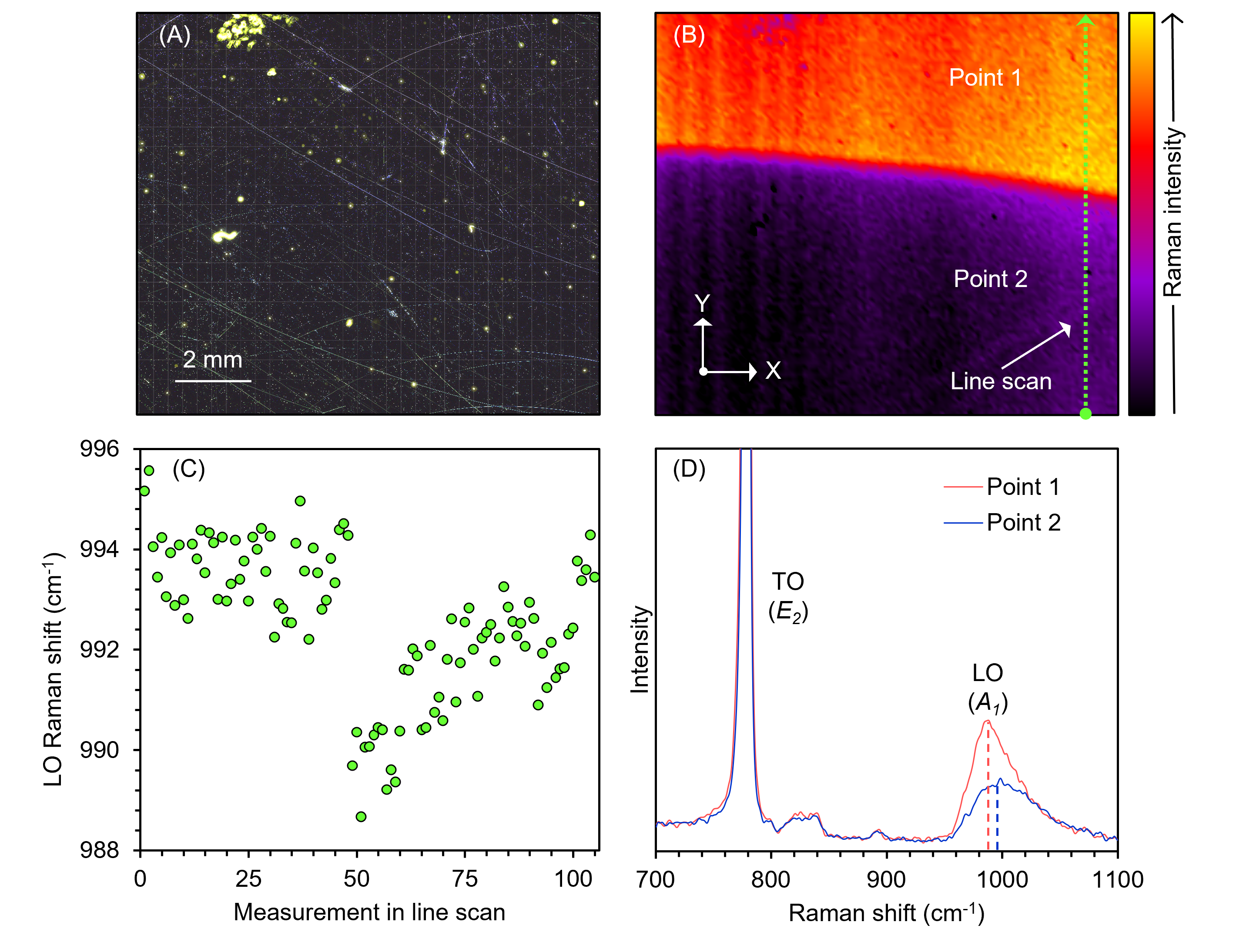
Figure 4. Raman imaging of the dopant concentration in an n-type 4H-SiC wafer. (A) A darkfield image of the Raman imaging area on the wafer. (B) A Raman intensity image of the LO phonon mode in SiC. (C) The peak position of the LO phonon mode recorded at each measurement along the green line scan in (B). (D) Spectra extracted from points 1 and 2 in (B).
The green arrow in the image in Figure 4B represents an extracted line scan. The panel in Figure 4C shows the peak position of the LO phonon mode recorded at each measurement along the line scan. The first measurement in Figure 4C indicates the measurement recorded at the bottom of the line scan in Figure 4B. It can be observed that in the image region where the LO Raman intensity is lower, the LO Raman shift is also higher on average when fit with a Voigt function. This is consistent with a higher nitrogen dopant/charge carrier concentration.
Figure 4D shows spectra extracted from the higher and lower charge carrier concentration regions. In the part of the sample with a higher charge carrier concentration, the LO phonon peak position and peak width are increased relative to the low charge carrier concentration region, and intensity is reduced. The profile of the TO band is unchanged.
Characterising defects in SiC wafers is crucial because they can cause failures in resulting electronic devices. These can be basal plane dislocations, stacking faults, point defects, or large defects such as polytype inclusions and foreign material micropipes. Raman spectroscopy is ideal because it is highly sensitive to structural changes in the material. Using 3D Raman imaging, it is possible to generate images that correlate morphological information about inclusions in X, Y, and Z with the chemical identity or a changing physical state.
We identified foreign crystals on the surface of the n-doped 4H-SiC wafer, Figure 5A, and used a combination of Raman spectral analysis and 3D mapping to gather more information. A 0.9 NA objective and a confocal pinhole diameter of 70 μm were used. A small confocal pinhole diameter reduces the collection volume within the sample and improves the axial spatial resolution during 3D mapping. XY and XZ planes from the 3D Raman map are shown in Figures 5B and 5C, respectively.
In Figure 5B, it is made clear that the two inclusions identified were chemically distinct from the surrounding wafer. The green false colouring corresponds to the Raman intensity of the TO (E2) band characteristic of 4H-SiC, and the red false colouring corresponds to the Raman intensity of a band at 795 cm-1, which was assigned to the TO (E1) band in 6H-SiC. The image of the XZ plane in the 3D Raman map, Figure 5C, which shows the defect indicated by the arrow in Figure 5B, provides information about the morphology of the inclusion. It is partly embedded within the 4H-SiC lattice and is a pipe-shaped crystal over 3 μm long.
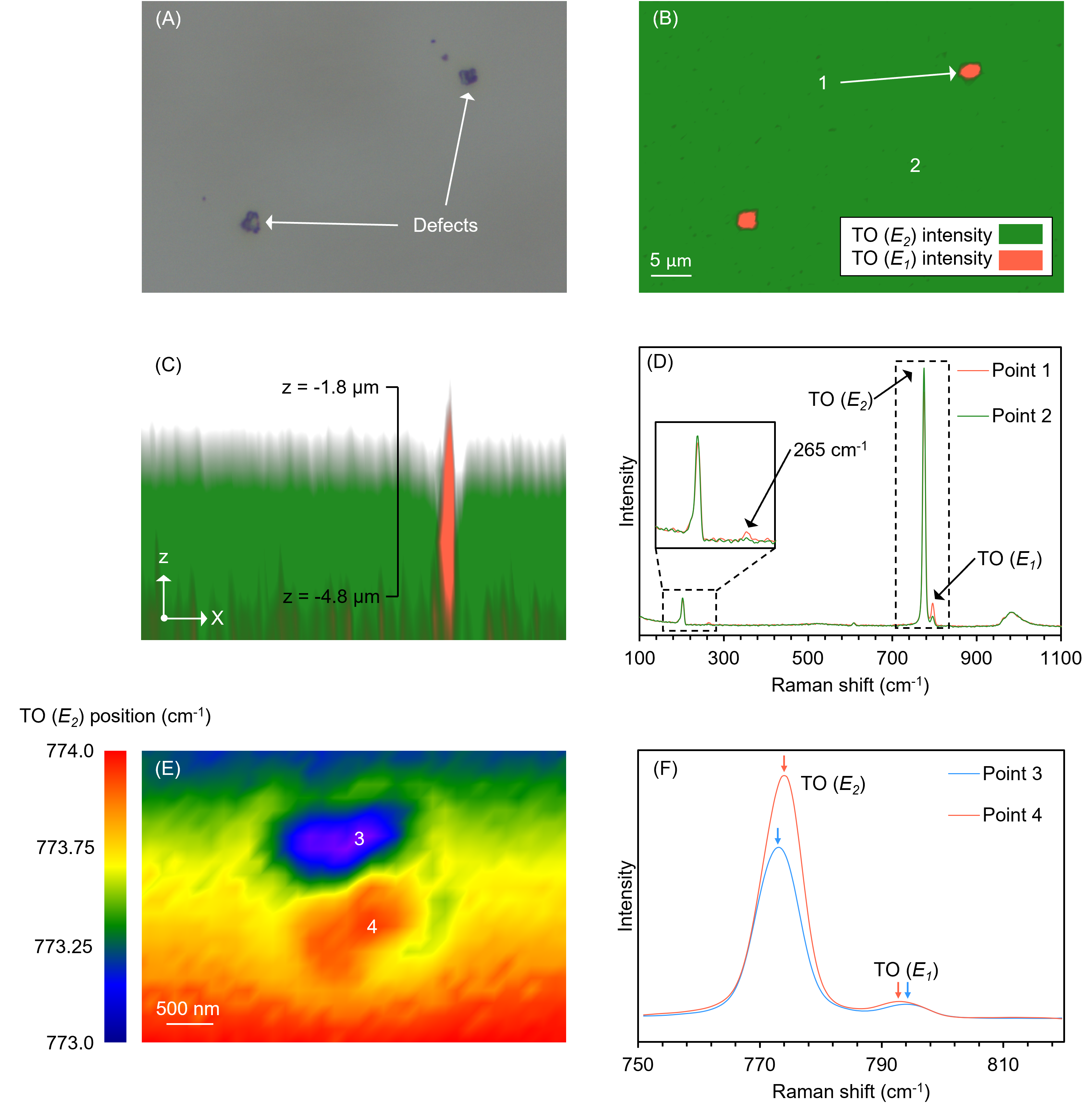
Figure 5. 3D Raman imaging of a defect in an n-type 4H-SiC wafer. (A) A brightfield image of the Raman imaging area on the wafer. (B) XY-plane from the 3D Raman image of the wafer and surrounding defects. (C) XZ-plane from the 3D Raman image. (D) Raman spectra from the wafer and defect. (E) Raman image of the TO (E2) band position across the defect in the top right-hand corner of the image in (A). (F) Extracted spectra from the points highlighted in (E).
Figure 5D shows spectra from the defect and the surrounding wafer. Compared to the surrounding wafer, the inclusion exhibits a lower-intensity TO (E2) band and a higher-intensity TO (E1) band. Also observed in the inclusion was a small band at 265 cm-1, assigned as the TA (E2) band of 6H-SiC.7
There was also significant variation in the Raman spectrum across the defect itself. Figure 5E shows a Raman image of the TO (E2) band position across the defect in the top right-hand corner of the Figure 5A image. Low (blue) and high (red) Raman shift clusters on the defect were observed, with a total variation between 773 cm-1 and 774 cm-1. These are points 3 and 4, respectively. Extracted spectra from these points also reveal variation in the position of the TO (E1) band, and the overall splitting between the two bands changing. In this example, 3D Raman imaging has revealed a considerable degree of structural complexity in this small inclusion within the wafer.
Raman spectroscopy is useful for characterising SiC semiconductor wafers and devices. In this Application Note, we have shown that Raman spectroscopy is sensitive to the structure of over 250 polytypes of the material and is, therefore, an excellent indicator of crystalline structure. Additionally, Raman imaging was used to detect changes in charge carrier concentration across the n-doped wafer analysed. Finally, 3D Raman imaging was applied to unveil the morphology and structural complexity of an inclusion embedded within the wafer.