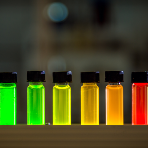
CdSe quantum dots (QDs) are widely used in bioimaging, displays, and photovoltaics due to their size-tuneable optoelectronic properties. Their adjustable bandgap makes them ideal for efficient solar energy harvesting.1
One potentially useful technique for integrating QDs into photovoltaic technologies is by embedding them in transparent matrices such as glass, which is particularly promising when the application benefits from glass as the medium, such as building-integrated photovoltaics (transparent solar windows, facades, greenhouses), Figure 1.2 Specific advantages of QD-photovoltaic glass include:
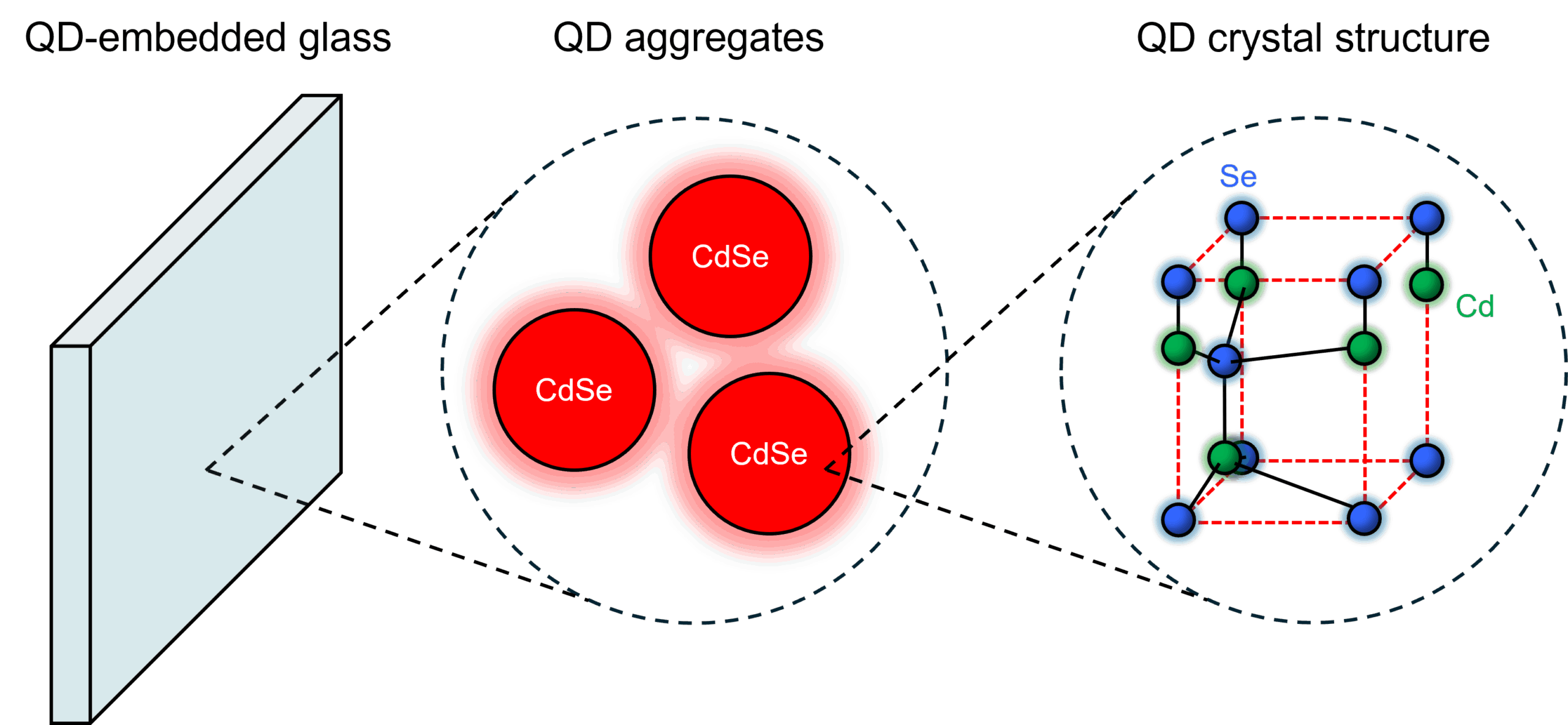
Figure 1. QD-embedded glass for building-integrated photovoltaics.
Given the high potential of QDs for next-generation solar technology, particularly building-integrated photovoltaics, it is crucial to understand their local structure and photophysical properties in such environments.
This Application Note demonstrates the correlative Raman, photoluminescence (PL), and fluorescence lifetime imaging microscopy (FLIM) analysis of CdSe QDs in a glass matrix using the RMS1000 Confocal Multimodal Microscope. By sequentially acquiring information about crystalline structure, electronic properties, and charge carrier dynamics, crucial structure-performance information can be obtained. These insights are only accessible through a system capable of seamlessly integrating Raman, PL, and FLIM, such as the RMS1000, which allows users to co-register spectral and time-resolved data within a single software environment.
The sample consisted of borosilicate glass doped with CdSe QDs. Raman, PL, and FLIM analyses were all performed on an RMS1000 system with a RaFLIM® upgrade, Figure 2.
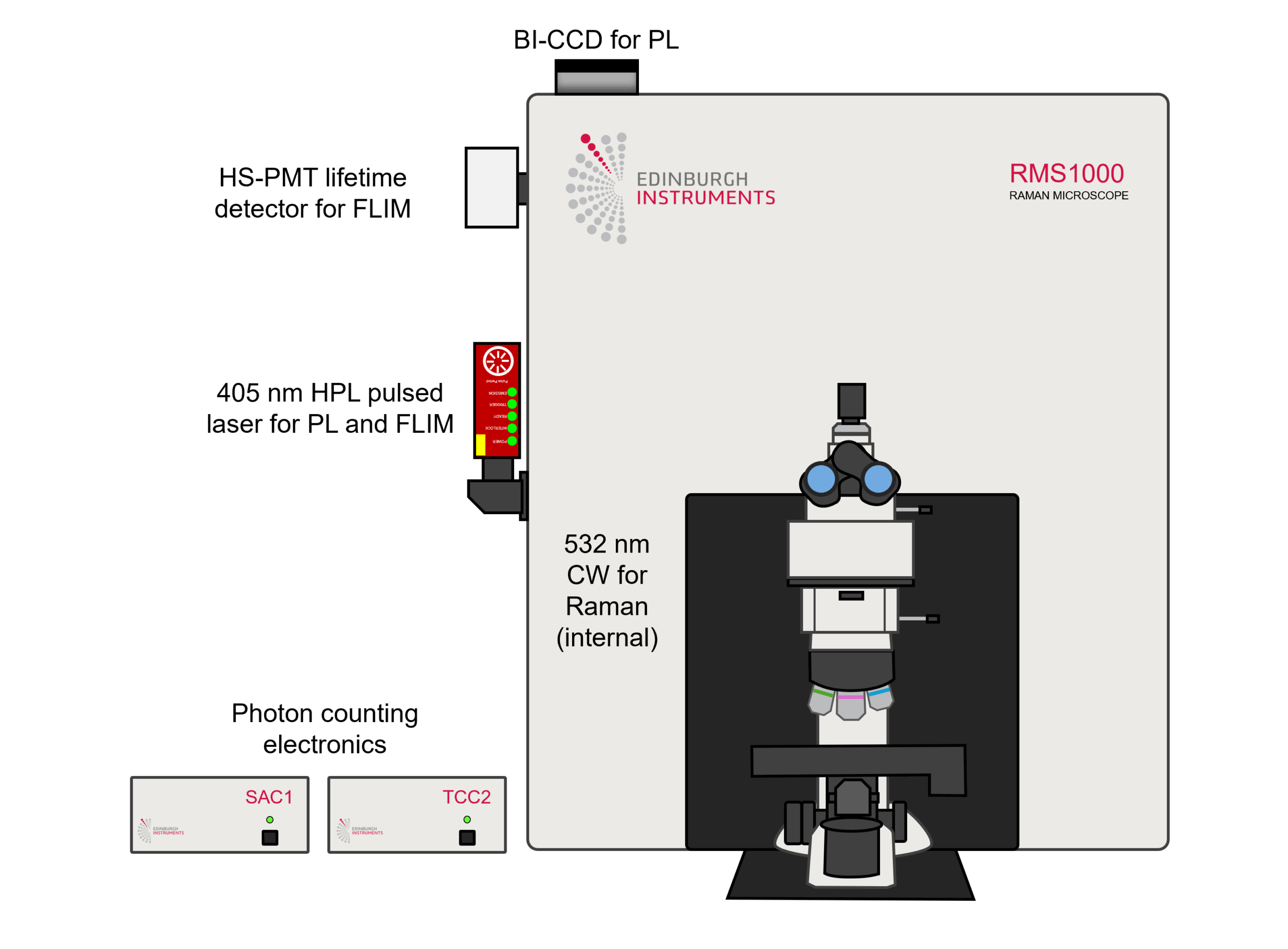
Figure 2. RMS1000 Confocal Multimodal Microscope with the RaFLIM upgrade.
2D imaging was performed on the same area of the sample for each technique. Mode-changing between images and subsequent data processing were all performed in Ramacle® software.
For Raman measurements, the system was equipped with an internal 532 nm CW laser and a back-illuminated CCD (BI-CCD).
For spectral PL and FLIM measurements, an externally coupled HPL-405 picosecond pulsed diode laser was used. For spectral PL, the laser was operated at 80 MHz and used as a , and the resulting PL emissions were detected using the BI-CCD.
For FLIM measurements, the laser was used at 10 MHz along with fluorescence lifetime electronics capable of both time-correlated single photon counting (TCSPC) and multichannel scaling (MCS), and a high-speed hybrid photodetector (HS-HPD). Decays were collected in TCSPC mode. The laser and detector combinations used for each technique are summarised in Table 1.
Table 1. The laser and detector combinations used for each imaging mode.
| Imaging Mode | Laser | Detector |
|---|---|---|
| Raman | 532 nm CW | CCD |
| PL | 405 nm HPL pulsed in quasi-CW mode | CCD |
| FLIM | 405 nm HPL pulsed | High speed hybrid photodetector (HS-HPD) |
The first spectroscopic technique used to analyse the sample was Raman imaging, Figure 3. The Raman image in Figure 3a shows the peak area of the dominant mode in CdSe QDs at 207 cm-1, a vibrational mode of A1 symmetry.4 The image shows that CdSe QDs are dispersed throughout the glass matrix in discrete aggregates. A representative Raman spectrum from a CdSe aggregate is shown in Figure 3b. The band at 420 cm-1 is attributable to second-order Raman scattering in CdSe, and the band at 490 cm-1 was assigned to the borosilicate glass matrix.5
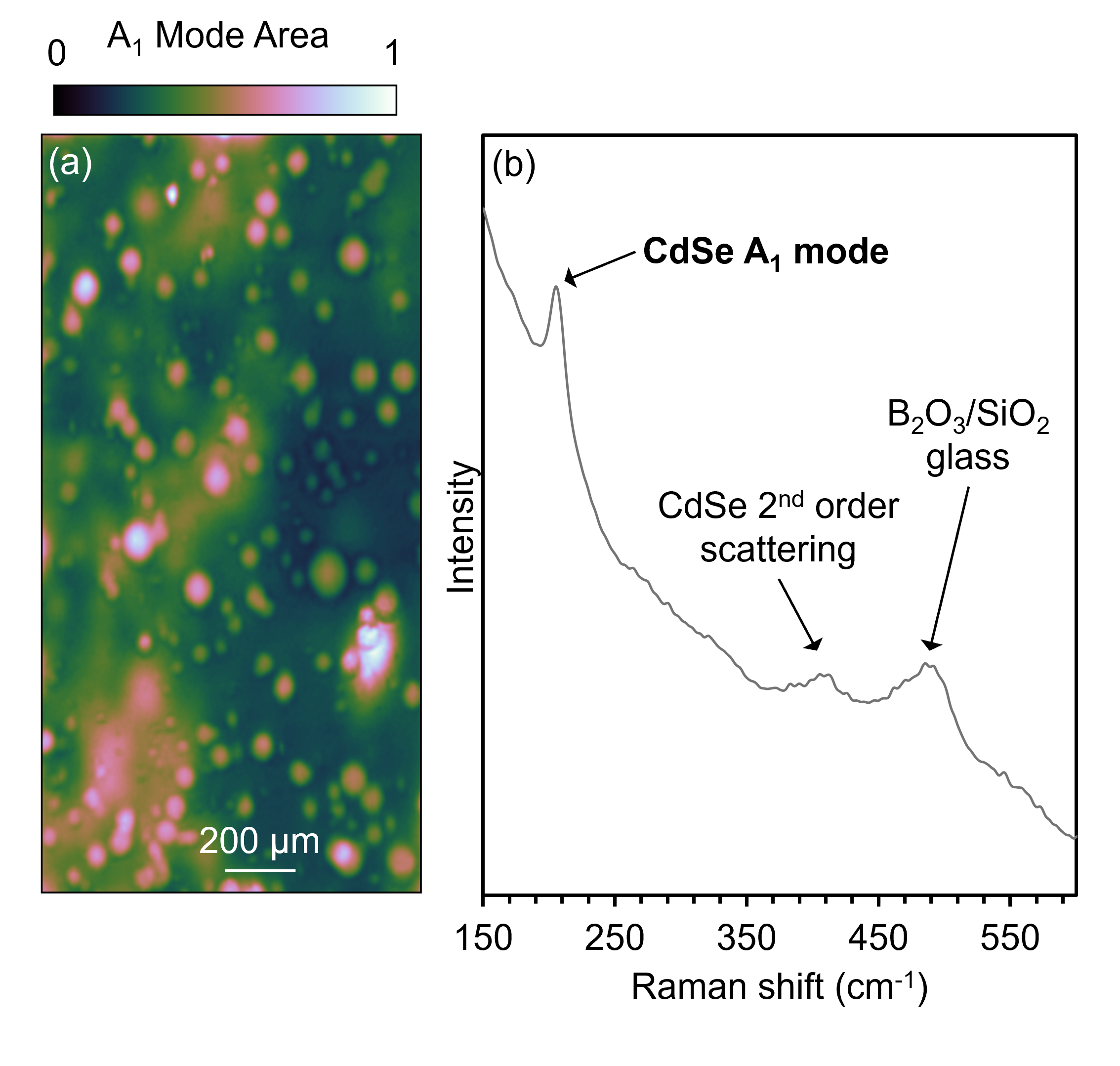
Figure 3. (a) Raman image of CdSe QDs in borosilicate glass using the peak area of the A1 symmetry mode to generate contrast. (b) A representative spectrum showing CdSe and borosilicate Raman signatures.
The Raman spectra of CdSe QDs are complex because they contain information about crystalline symmetry (wurtzite and zincblende are possible), size-dependent phonon confinement, and matrix-induced strain, all of which will impact optoelectronic behaviour.6 In photovoltaic glass, this structural information helps link QD synthesis and embedding protocols with device performance, enabling rational design of next-generation luminescent solar materials.
Spectral PL imaging in Figure 4 reveals that the CdSe QDs emit strongly at 504 nm. Using a 405 nm excitation in the near-UV, these QDs absorb high-energy light and reemit it at longer wavelengths.
This spectral downconversion can improve solar cell efficiency by converting UV photons into harvestable visible light, benefiting devices like silicon solar cells that have limited UV absorption.
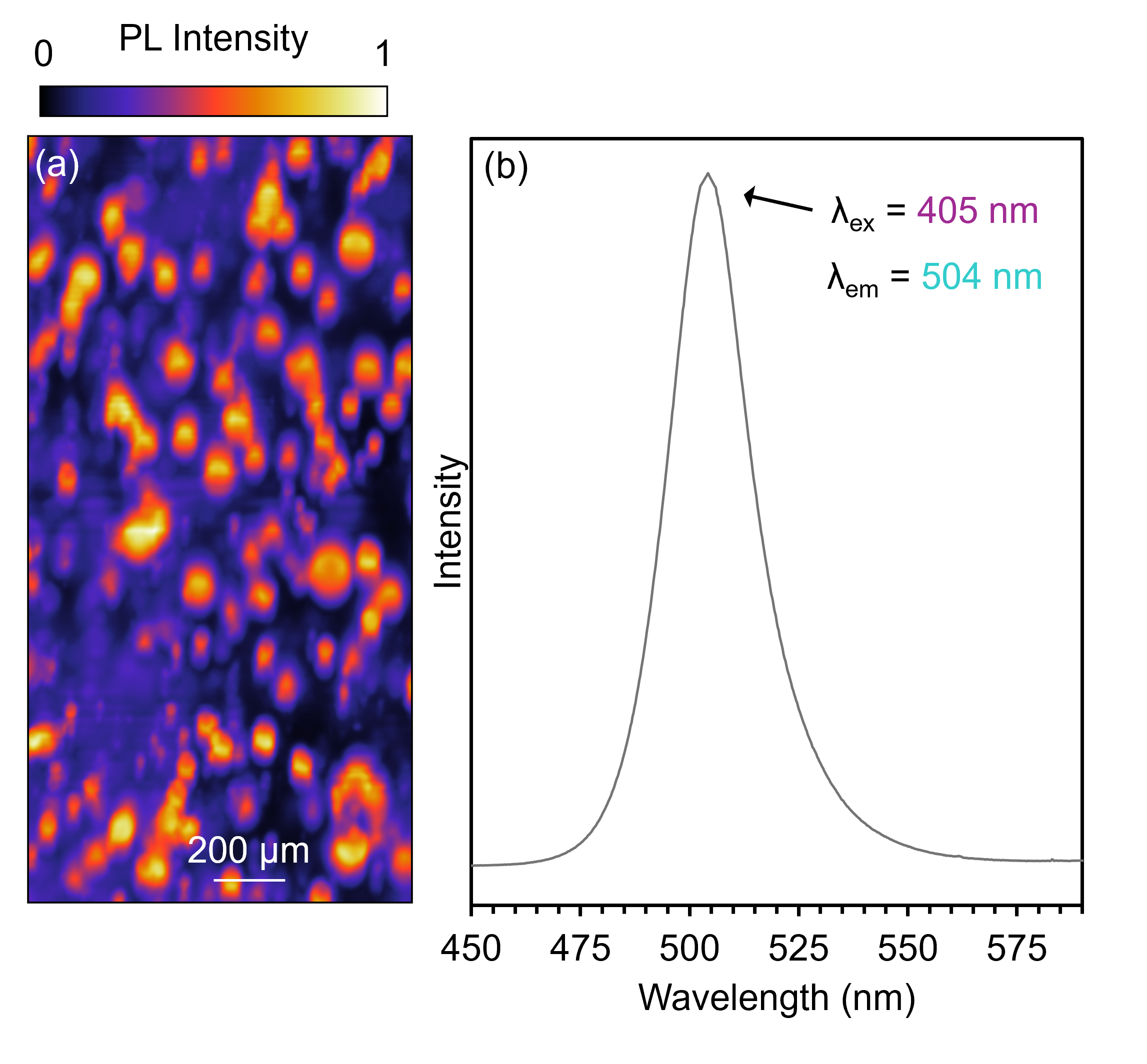
Figure 4. (a) PL image of CdSe QDs in borosilicate glass using the peak intensity of the 504 nm band. (b) A representative PL spectrum showing CdSe emission.
While PL reveals optical emission efficiency and provides information about the bandgap of the material, it does not capture the dynamics of charge carrier relaxation or non-radiative processes. For that, analysis using FLIM is required.
The image in Figure 5a shows intensity-averaged lifetime variations (3.1 to 4.3 ns) across CdSe QDs in glass, which can be linked to radiative and non-radiative recombination processes. Longer lifetimes indicate efficient radiative decay; shorter lifetimes suggest defects or matrix interactions enabling non-radiative decay pathways.7
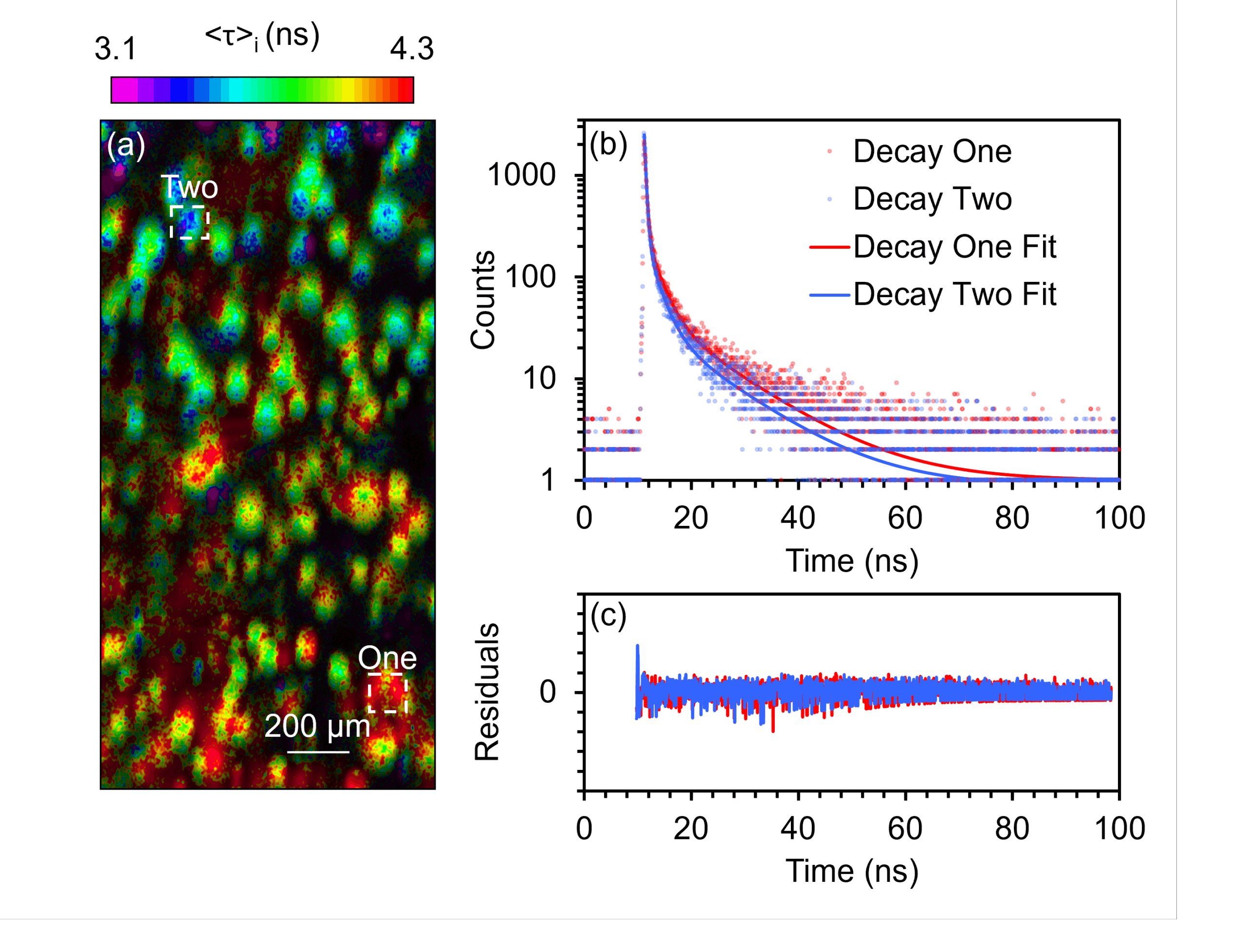
Figure 5. (a) Intensity-averaged lifetime (<τ>i) image of CdSe QDs in borosilicate glass. (b) Fitted tri-exponential fluorescence decay curves for two distinct regions (“One” and “Two”) identified in (a). (c) Corresponding residuals for the decay curve fits, indicating fit quality.
Figures 5b and 5c present the fluorescence decay curves and their corresponding residuals from two distinct regions, “One” and “Two,” highlighted in the lifetime map. The tri-exponential nature of these decays, Figure 5b, is typical for QDs, reflecting the inherent heterogeneity in QD size, surface passivation, and local environment within the glass matrix. The excellent fit between the experimental data points and the multi-exponential models, as indicated by the randomly distributed residuals around zero in Figure 5c, validates the accuracy of the lifetime analysis.
This Application Note effectively demonstrates the power of correlative Raman, PL, and FLIM imaging, performed on the RMS1000 Confocal Multimodal Microscope, for the in-depth characterisation of CdSe QDs embedded in glass. By linking local crystal structure to emission properties and charge carrier dynamics within the same sample region, this correlative approach can offer crucial insights into structure-function relationships. This approach is essential for understanding and optimising QD behaviour, paving the way for advanced photovoltaic glass and other next-generation optoelectronic materials.
Contact us to learn how the RMS1000 can help you gain these critical insights and accelerate your photovoltaic materials development.