Photoluminescence (PL) is a valuable technique for probing the electronic properties of semiconductors such as silicon. While PL is typically studied using dedicated PL systems, Raman microscopes equipped with NIR-sensitive detectors can also efficiently capture silicon PL, providing an integrated solution for both Raman and PL analysis.
This Technical Note examines how detector choice, specifically between CCD and InGaAs, affects the quality and reliability of silicon PL measurements. A general introduction and comparison of these two detector types is given in this Spectral School article: Detectors for Raman Spectroscopy.
Understanding how silicon emits PL is key to measuring it effectively. In materials like silicon, light emission occurs when an electron and a hole recombine. However, silicon is an indirect bandgap semiconductor (Figure 1). This means the electron requires the absorption or emission of a phonon to conserve momentum in k-space.1
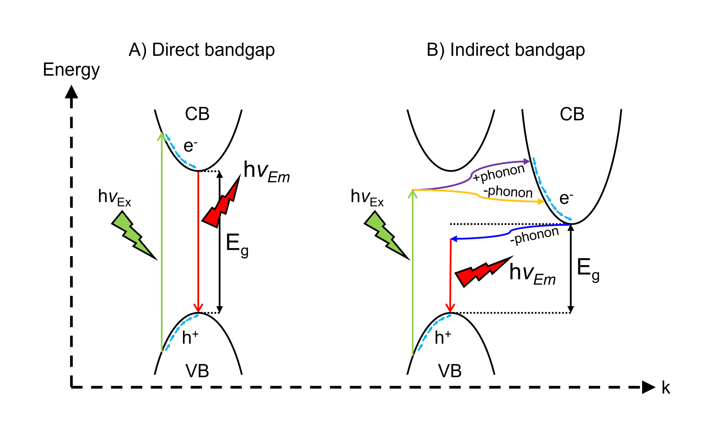 Figure 1. Schematic diagrams illustrating the fundamental differences between PL in (A) direct and (B) indirect bandgap semiconductors.
The indirect nature of silicon’s PL means it’s observed at a slightly longer wavelength (lower energy) than its theoretical bandgap, typically around 1136-1148 nm (compared to a bandgap of 1107 nm) (Table 1). This PL signal is highly valuable for probing silicon’s electronic properties.
Table 1. Comparison of bandgap energy and PL emission of silicon.2
| Property | Energy (eV) | Wavelength (nm) |
|---|---|---|
| Bandgap | ~1.12 eV | ~1107 nm |
| Typical PL Emission | ~1.08 – 1.10 eV | ~1136 – 1148 nm |
Silicon PL can be detected and imaged using a Raman microscope configured for NIR detection. However, accurately capturing the PL emission of silicon depends on the detector used. For NIR measurements on a Raman microscope, a CCD or an InGaAs detector can be used. In this section, we compare silicon PL detected using an RM5 equipped with a 532 nm laser and both a CCD and an InGaAs detector.
CCD detectors exhibit high quantum efficiency (QE) in the visible region but begin to drop off significantly around 1000 nm. In contrast, InGaAs detectors are specifically designed for NIR sensitivity and maintain high QE across the 1000–1600 nm range. This difference strongly influences both the intensity and apparent spectral position of the measured PL signal, as is shown in Figure 2, which compares normalised PL spectra from the same point on a silicon wafer acquired using a 532 nm laser and each detector.
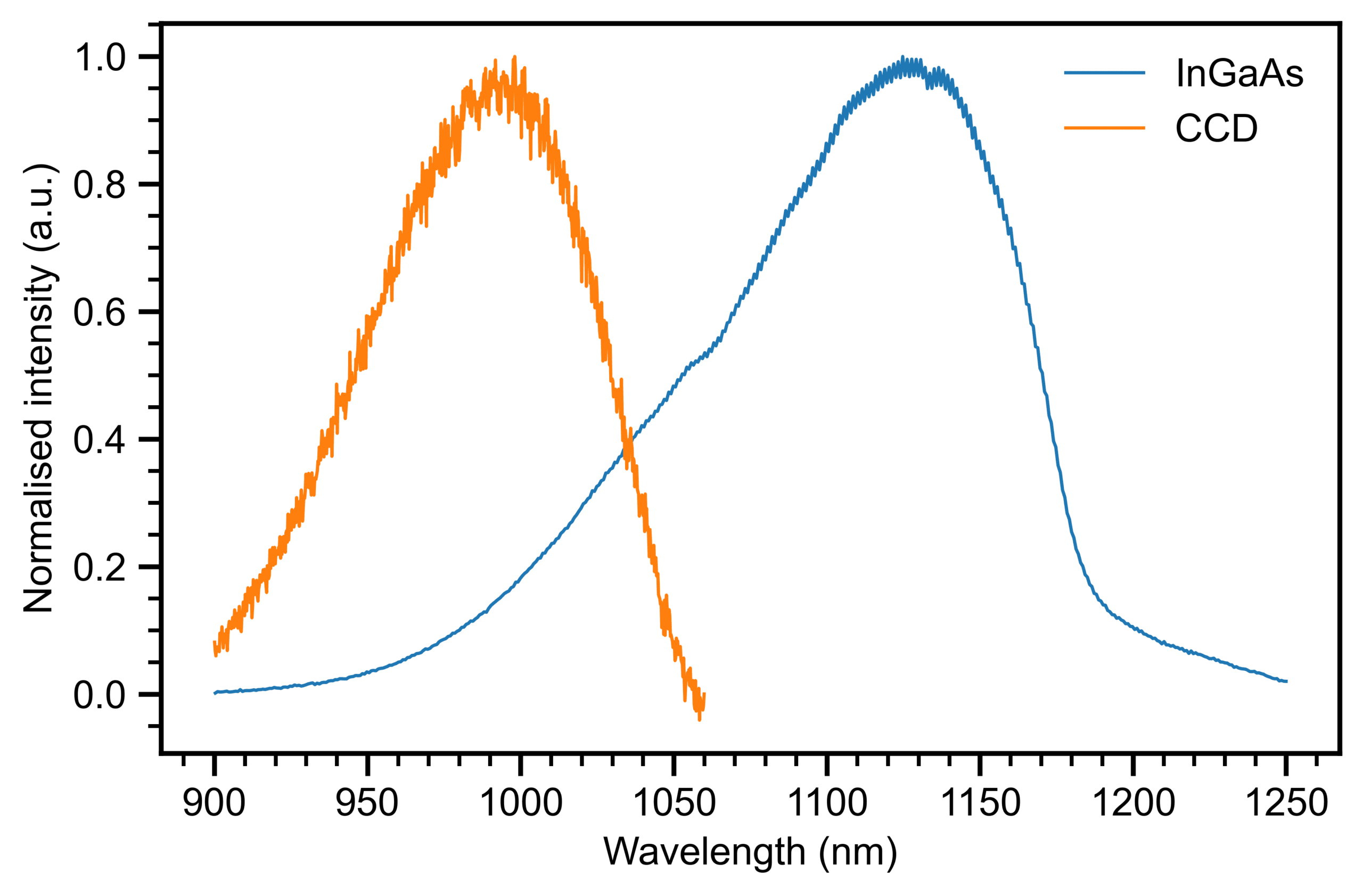
Figure 2. PL spectra acquired from the same point on a silicon wafer with a CCD (orange) and an InGaAs detector (blue). In both spectra, a 532 nm laser was used.
When an InGaAs detector is used, the PL peak is centred around 1120 nm, which reflects the intrinsic emission of silicon close to the bandgap energy. When a CCD is used, however, the PL peak observed is centred around 980 nm. The blueshift observed in the CCD most likely arises because of the detector’s rapidly falling QE in the NIR, causing the signal to appear skewed towards a shorter wavelength. Table 2 shows a comparison of the two detectors for silicon PL.
In practical terms, CCD-based PL maps are still valuable, especially for relative intensity comparisons across a wafer, but not reliable for absolute peak position or shape. When an NIR laser, such as 830 nm, is used with a CCD, Raman and PL can be detected simultaneously in a single scan. With a visible laser, simultaneous detection of Raman and PL is possible with Extended Scan mode, but this is, of course, slower. With an InGaAs, Raman and PL can only be detected sequentially, as a change in optics would be required to switch imaging modes, but the trade-off is greater spectral accuracy.
Table 2. Comparison of CCDs and InGaAs arrays for silicon PL detection.
| Detector | NIR Sensitivity | Spectral Accuracy | Raman and PL? |
|---|---|---|---|
| CCD | Limited to ~ 1000 nm | Low bandgap accuracy, relative intensity changes in imaging are possible | Simultaneously, when an NIR laser is used |
| InGaAs | High: 1000 nm – 1600 nm | Accurate in terms of bandgap and relative intensity changes in imaging | Sequential only |
Silicon PL can be effectively measured using a Raman microscope equipped with suitable detection hardware. The ability to acquire PL from silicon using either a CCD or an InGaAs detector opens flexible pathways for characterisation, depending on the measurement goals.
The detector choice has a direct impact on both spectral accuracy and the practical workflow of analysis:
A clear understanding of the strengths and limitations of each detector enables the selection of an approach best suited to the specific analytical objective, whether identifying defects, monitoring processing-induced variations, or validating material quality via PL.