Welcome to Edinburgh Instruments’ blog, celebrating our work in Raman, Photoluminescence, and Fluorescence Lifetime Imaging. Every month, we aim to highlight our pick for Map of the Month to show how our Raman and fluorescence spectrometers can be used to reveal all the hidden secrets in your samples.
This month, we are very excited to be hosting our first Webinar in the Spectroscopy in Action Series, covering multimodal microscopy and 2D materials. With 2D materials in mind, we thought it would be fitting to highlight graphene in this Map of the Month, the material that sparked over a decade of innovation and discovery (so far!) within the field. We are highlighting a case study from our Graphene eBook, in which we image tensile strain on a graphene film deposited atop a defective silicon wafer.
Strain in materials causes bond lengths to change, altering their vibrational frequencies and the material’s properties under investigation. Raman spectroscopy is, therefore, highly sensitive to strain. In graphene, strain is associated with a frequency change in the key vibrational modes. This is reflected in the Raman shift of the G and 2D bands, meaning the position of these bands can be used to create a strain map of the graphene surface.
A monolayer film grown on a silicon wafer with several fissures was mapped to track strain in the graphene using Raman microscopy (Figure 1). Imaging was performed on an RM5 with a 532 nm laser and an 1800 gr/mm grating to ensure that subtle changes in peak position could be resolved. Peak position imaging was performed in Ramacle®.
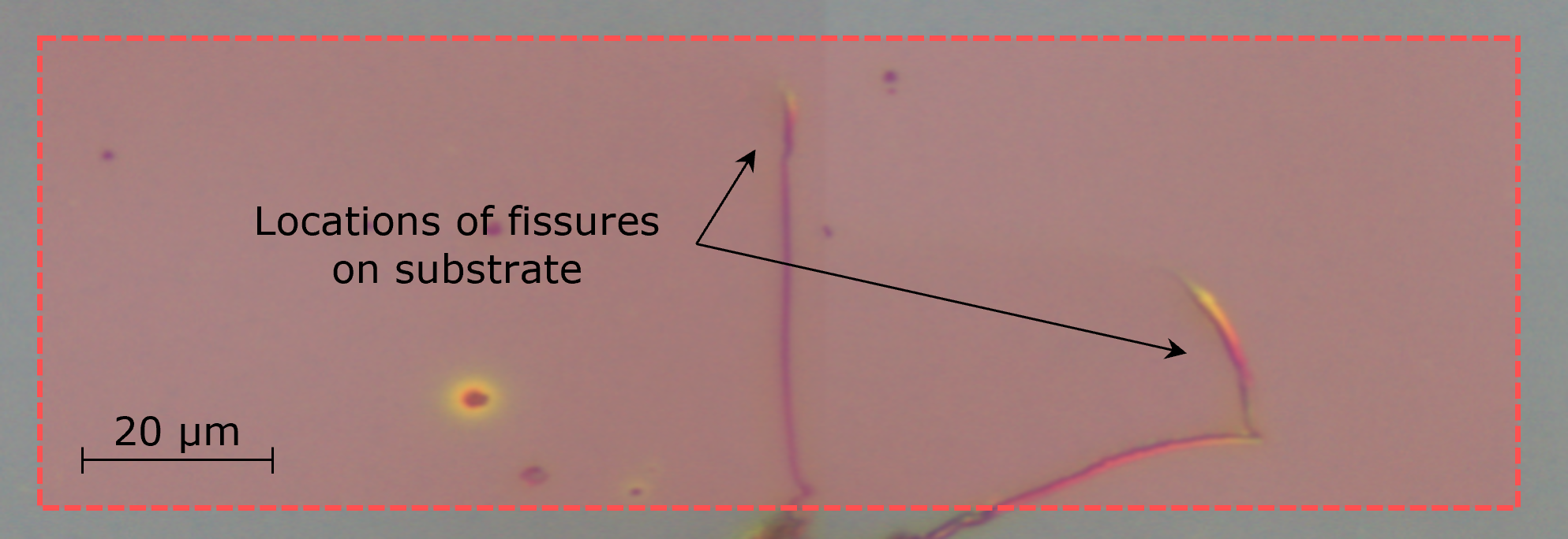
Figure 1. A brightfield image of a graphene film on a silicon wafer with the Raman imaging area overlaid in red.
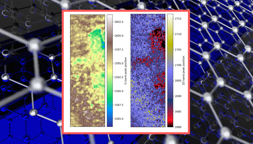
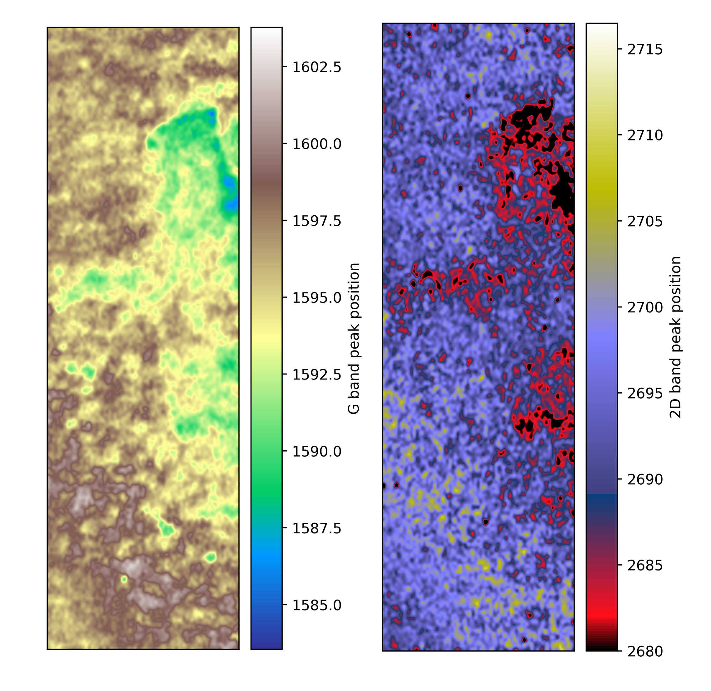
The area imaged on the sample contained two fissures on the underlying silicon substrate, hypothesised to affect the mechanical properties of the graphene film deposited on top and induce strain. Strain is associated with positional changes in both the G and 2D bands; here, both band positions were tracked during imaging.
This image in Figure 2 indicates that there is a decrease in the Raman shift of the G band in the regions where the graphene is laid atop the fissures. Tensile strain causes the elongation of molecular bonds, lowering the energy of the mode, which is proportional to the Raman shift. This image suggests that the fissures create tensile stress in the graphene because it is stretched.
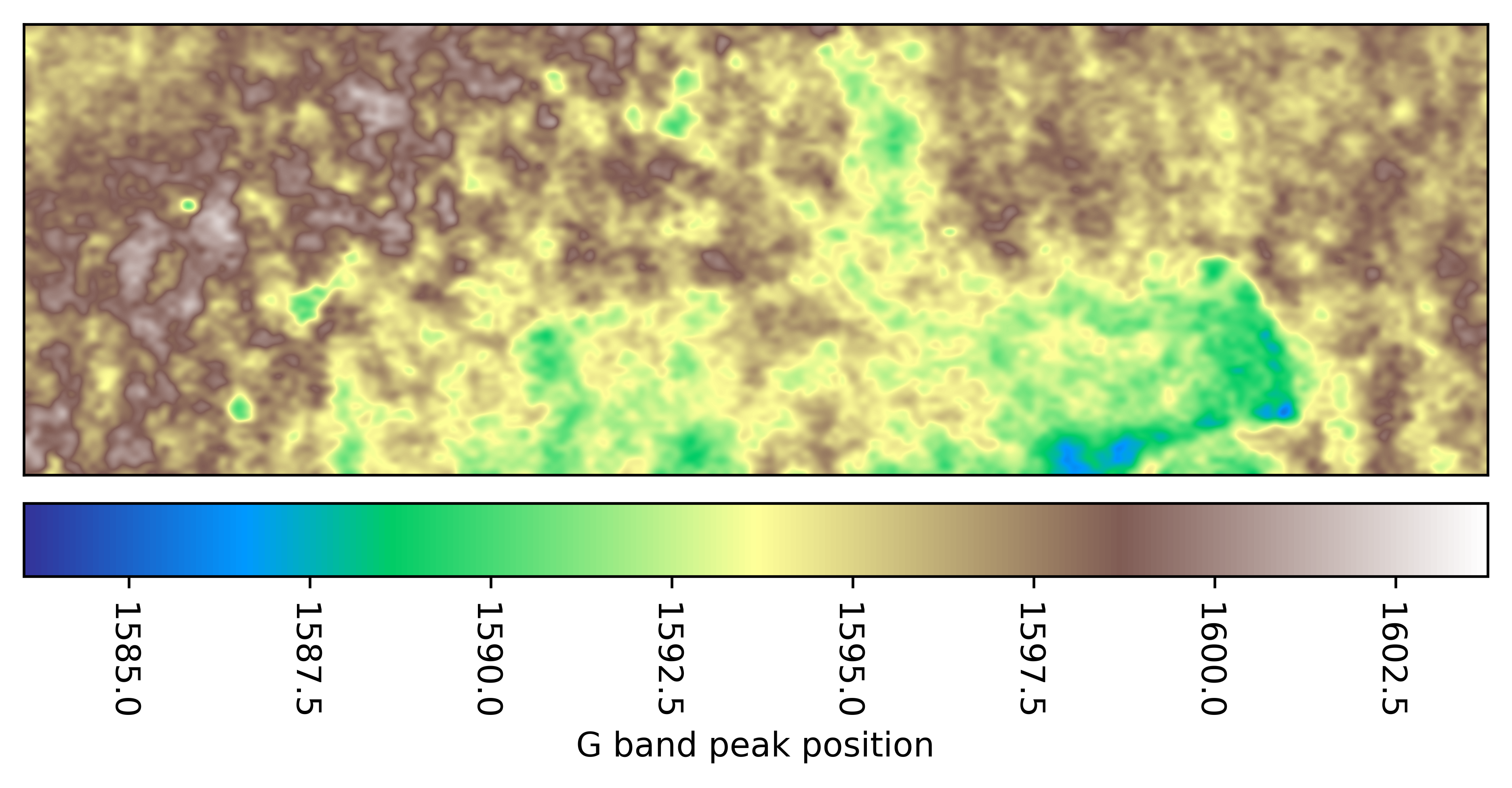
Figure 2. Peak position Raman image of the G band of graphene.
Further evidence of tensile strain is shown in Figure 3, which is an image of the 2D band position across the sample. Again, the lower Raman shift of this band atop the fissures is indicative of strain.
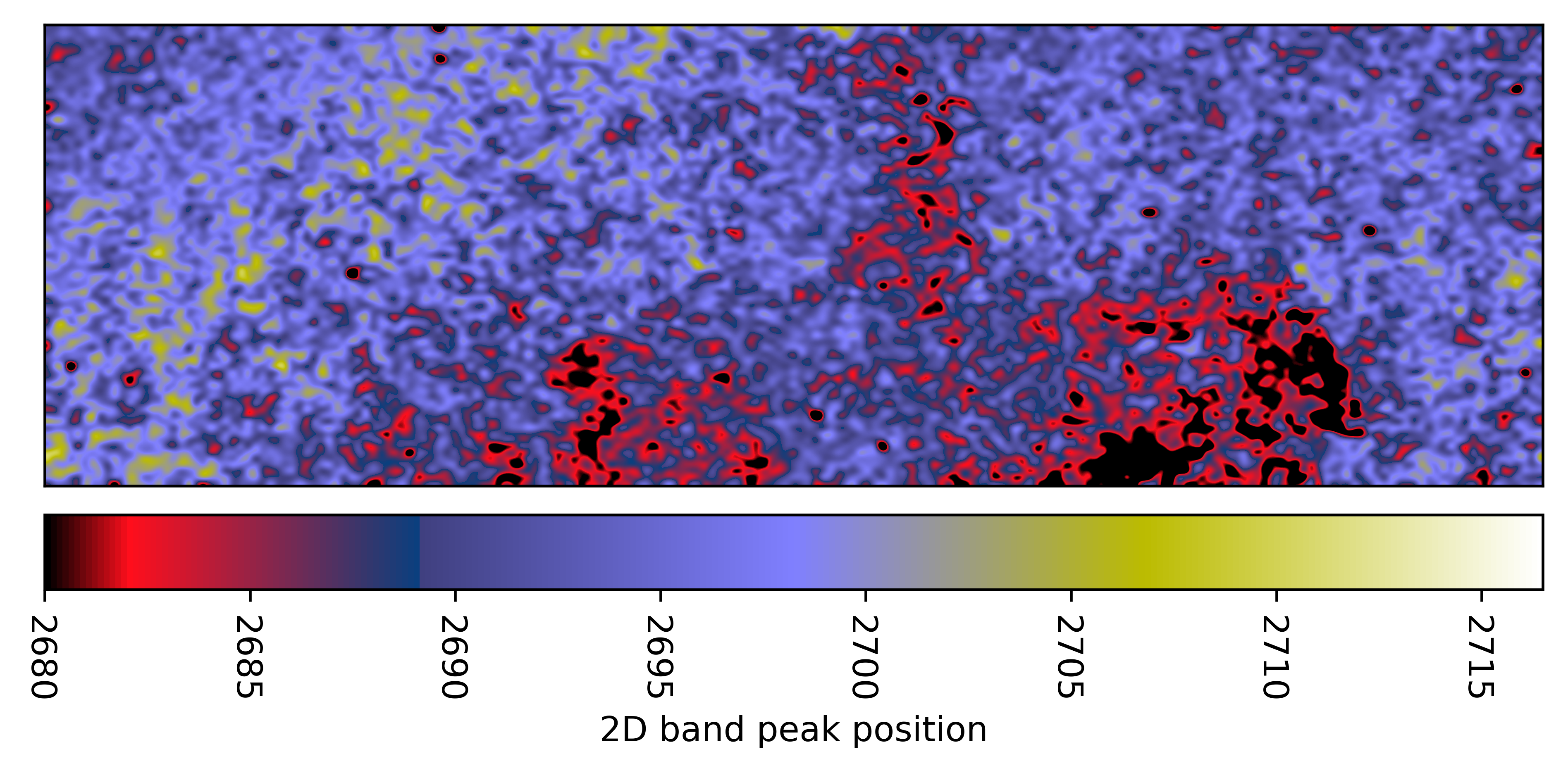
Figure 3. Peak position Raman image of the 2D band of graphene.
Spectra from strained and unstrained regions are shown in Figure 4. They show that both bands are shifted simultaneously.
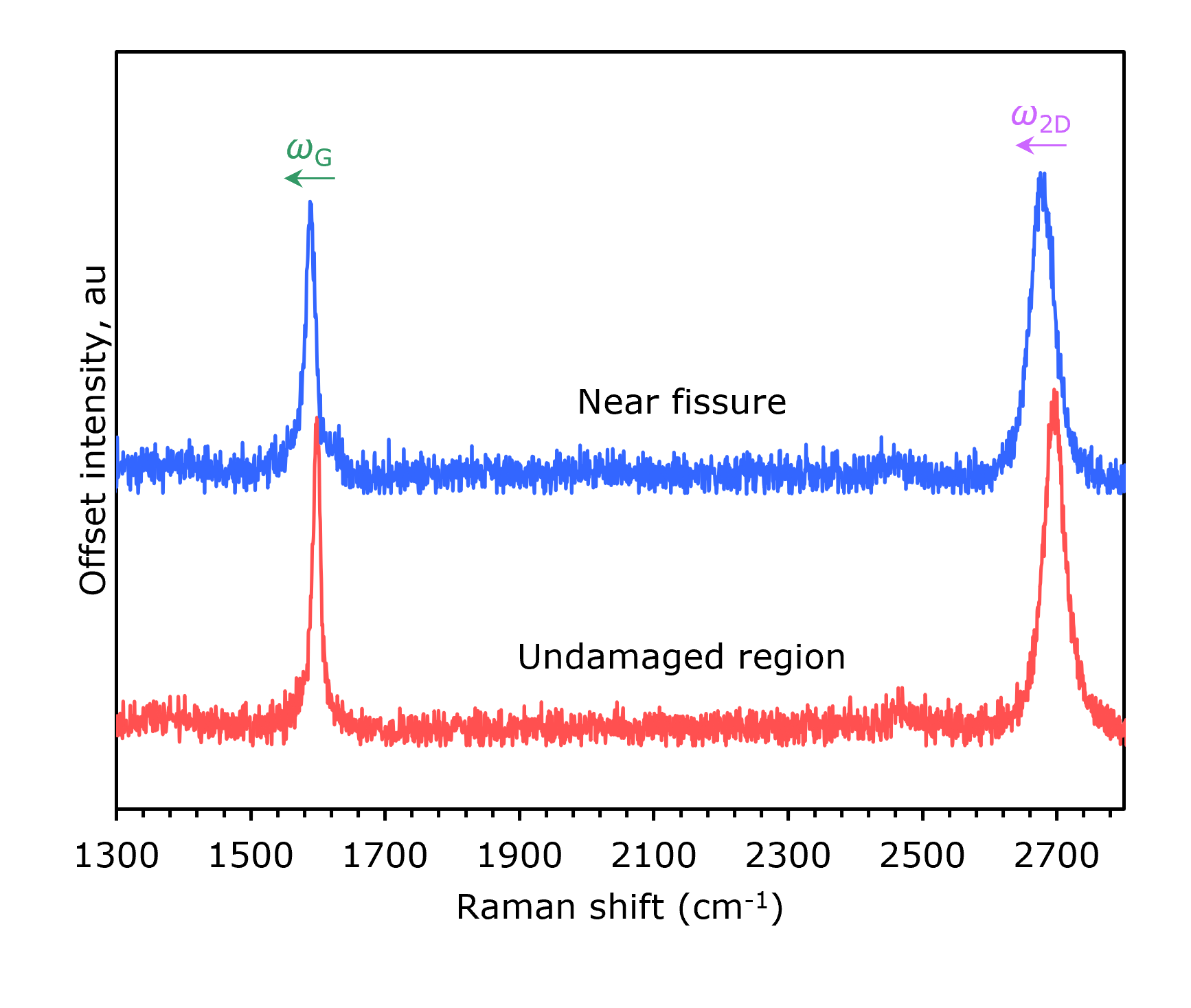
Figure 4. Raman spectra from strained and unstrained parts of the graphene film.
So there we have it! Peak position Raman imaging was used to track strain on a graphene film. Parts of the film overlaid on fissures on the silicon substrate exhibited reduced Raman shift G and 2D bands, and imaging of the band positions showed that the fissures were causing tensile strain locally within the film.