Two-dimensional (2D) materials are poised to be essential in next-generation electronics, including emerging quantum computers and artificial intelligence chips. Their appeal lies in their ultra-small size and unique, tuneable properties—such as superconductivity in some materials—making them ideal for advancing technology that demands faster, more efficient performance while minimising space. So, what are they?
2D materials are atomically thin, consisting of a single layer of atoms arranged in a plane, much like a sheet of paper but on an atomic scale. Whilst their 3D counterparts make up the bulk of our everyday world, in 2D, they reveal a hidden universe of possibilities. But how do these atomic sheets unlock such incredible potential?
Think of electrons like ping pong balls. In 3D, they have plenty of room to bounce around freely in all directions, bumping into each other but mostly moving as they please. This gives 3D materials their familiar properties. In 2D they are confined to a tabletop, their movement is restricted to only rolling forward, backward, left, and right. On the tabletop, the ping pong balls roll faster, collide more often, and move in sync, leading to surprising, new and exciting properties. This phenomenon is known as quantum confinement, and it occurs when the motion of a particle is confined to a space that is smaller than its wavelength
In this blog we’ll explore the original 2D material which started the revolutionary field – graphene. We’ll then introduce the future faces in 2D materials, and how Edinburgh Instruments can support this research.
Graphene – The OG
Graphene was the first 2D material to be isolated – although the theoretical existence of single layer of graphene had been discussed since the 1940s, it wasn’t until 2004 that Andre Geim and Konstantin Novoselov isolated the material at the University of Manchester.
On Friday evenings, instead of going to the pub, the two researchers used their free time to conduct experiments that their normal schedule wouldn’t allow. Using sticky tape to remove some graphite from a larger bulk piece, they realised that some of the flakes on the tape were thinner than others. After repeatedly separating the flakes, they managed to obtain a layer of graphite just one atom thick. They had just isolated graphene!

Figure 1. A lump of graphite, a graphene transistor, and a tape dispenser. Donated to the Nobel Museum in Stockholm by Andre Geim and Konstantin Novoselov in 2010.
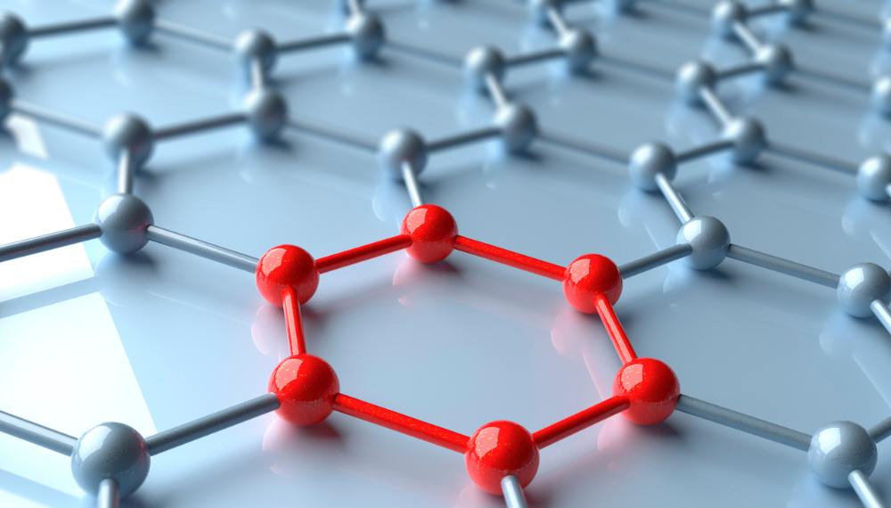
Since then, graphene research has boomed, and it has become colloquially known as ‘The Wonder Material’. Graphene’s structure is defined by a hexagonal lattice of carbon atoms, forming a single atomic layer (Figure 2). This single-atom thickness makes graphene the thinnest material known, contributing to its exceptional strength and flexibility. The strong covalent bonds between the carbon atoms within this lattice give rise to its remarkable ability to conduct both electricity and heat efficiently. The uses of graphene are extensive and include various application areas in high-capacity batteries, supercapacitors, photodetectors, semiconductors, bioengineering, microelectronics, batteries, and composites.
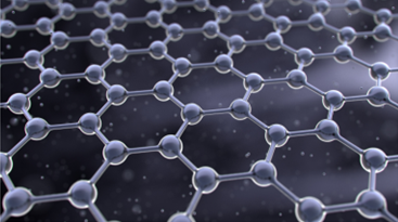
Figure 2. Hexagonal structure of graphene.
Within biomedical applications, graphene has been shown to be used in creative ways in the detection of disease states, enhancement of drug delivery systems and even in the ever-growing field of smart implants. In 2024, the world’s first human-graphene based brain computer interface procedure was performed at Salford Royal Hospital. Currently in the clinical trial phase, the smart implant aims to demonstrate graphene’s superiority over other materials in determining brain functionality in awake and asleep states.
New Kids on the Block
So what came next, and what is on the horizon? Despite his own discovery, Professor Sir Andre Geim was quoted in Nature in 2013 as saying ‘It is probably fair to say that research on ‘simple graphene’ has already passed its zenith.’ Geim saw graphene’s research moving forward into real-world applications, thus opening the research field to investigate new forms of 2D materials. Let’s meet the key players …
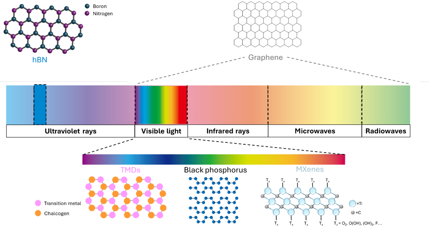
Figure 3. Detection ranges of different 2D materials on the electromagnetic spectrum.
Mxenes
First reported in 2011, 2D carbides and nitrides of transition metals have gained a surge of interest in the past decade. These materials, now known as MXenes, are poised to become the foundational building blocks of future materials and devices, ushering in a new era of technological advancement.
MXenes, with the formula Mn+1XnTx (where n = 1-3), consist of transition metal atoms (M) interleaved by carbon and/or nitrogen (X). The surface termination groups (Tx) such as -F, -O, -OH, or -Cl enhance their properties, offering versatility for various applications. These materials stand out among other 2D materials due to their unique combination of metallic conductivity, hydrophilicity, and tuneable surface chemistry, making them promising for energy storage, sensing, and other advanced technologies.
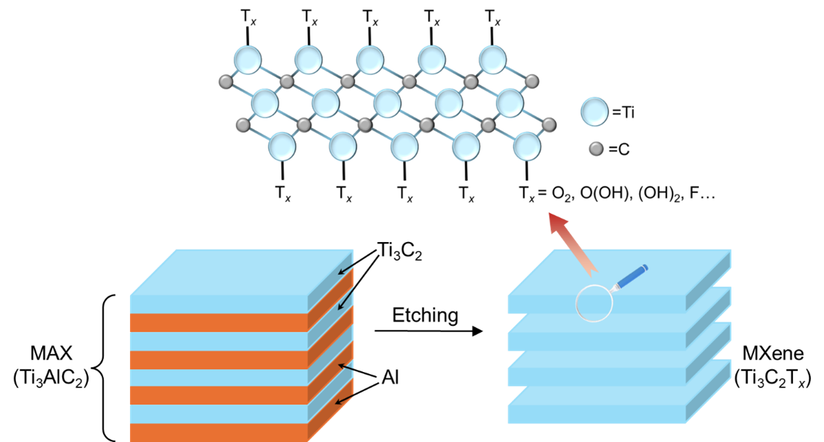
Figure 4. MXene preparation by MAX phase etching.
MXenes demonstrate exceptional performance in electromagnetic interference (EMI) shielding. EMI shielding, the process of blocking unwanted electromagnetic radiation, is essential for protecting sensitive components and preventing signal degradation. In particular, within aircrafts EMI shielding allows for reliable operations without disruptions from electromagnetic interferences. Mxenes potentials are maximised when combined with materials like polymers and fibres, paving the way for next-generation electronic devices that are less susceptible to interference.
TMDs
Transition-metal dichalcogenides (TMDs) are typically semiconducting materials offering a remarkable range of tuneable properties, making them ideal for tailoring materials to specific needs. This tunability arises from their varied crystal structures, defined by the stacking of transition metal atoms (M) and chalcogen atoms (X) in an X-M-X configuration. This structural diversity allows scientists to fine-tune TMDs for a variety of applications.
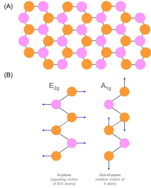
Figure 5. (A) TMD structure X-M-X; M=Transition Metal (e.g., Mo) X=Chalcogen (e.g., S). (B) Illustration of Raman active modes.
For decades, silicon has reigned supreme in the chip industry, its semiconductor properties driving technological progress. But with the rise of power-hungry technologies like 5G and artificial intelligence, the demand for even better chips has never been greater. These advancements require significantly higher processing power and consume substantially more energy.
TMD-based chips are being actively researched as a potential solution, offering a bridge to the future of computing. TMDs, with their unique atomic arrangement and electronic band structure, offer the potential for greater electron mobility and more efficient control of electrical current compared to silicon. This translates to the possibility of reduced power consumption and increased processing speeds, did you know that a typical request to Chat GPT consumes 10 times as much energy as a conventional Google search?! Researchers anticipate that TMD-based chips could use approximately 40% less power and perform up to 1000 times faster than current silicon-based chips.
Phosphorene
Graphene sparked the 2D materials revolution, and TMDs broadened the landscape. But there’s another player entering the field, a material with the potential to bridge the gap between the two: phosphorene, which was first exfoliated from black phosphorus into monolayers in 2014.
Phosphorene boasts a unique combination of properties, including a direct band gap and high carrier mobility, setting it apart from other 2D materials. Like graphene, it has a layered structure, but its distinct arrangement (see Figure 6, showing the four-atom unit cell with both zigzag and armchair structures) gives it a special edge.
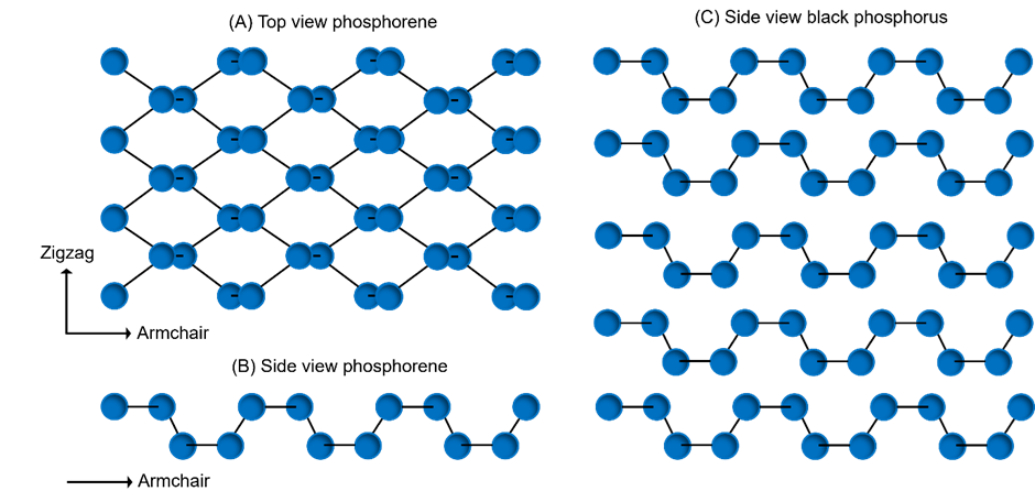
Figure 6. (A) Top and (B) side views of single-layer phosphorene with arrows showing zigzag and armchair directions. (C) Black phosphorus structure.
Phosphorene shows great potential for solar cells and batteries. Its direct band gap facilitates efficient light absorption, and its high capacity allows for increased charge storage. Doping or creating composite materials with phosphorene can further enhance its performance, improving efficiency and stability.
hBN
Hexagonal boron nitride (hBN), or “white graphene,” is a 2D material notable for its robust electrical insulating properties. Its large band gap makes it an excellent dielectric, and its corrosion resistance and thermal/chemical stability further enhance its utility. Structurally, hBN has a hexagonal lattice (Figure 7) of covalently bonded boron (blue) and nitrogen (purple) atoms.
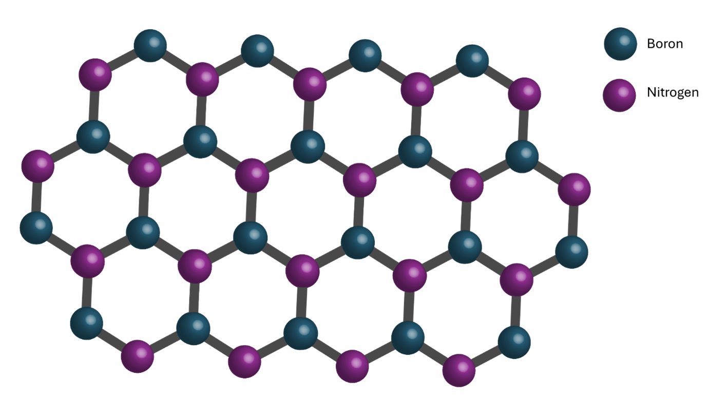
Figure 7. h-BN 2D structure.
hBN is finding increasing use in the realm of next-generation electronics, particularly in the development of high-performance transistors, e.g. MOSFETS and FinFETS. As transistors shrink in size and operate at higher frequencies, the need for effective insulating materials becomes paramount. hBN, with its exceptional electrical insulating properties and large band gap, serves as an ideal gate dielectric in these advanced transistors. This insulation is crucial for preventing current leakage and ensuring efficient device operation. Moreover, hBN’s high thermal conductivity helps to dissipate heat generated during transistor operation, contributing to improved device stability and longevity. By incorporating hBN into these critical components, manufacturers can create transistors that are smaller, faster, and more reliable, paving the way for more powerful and energy-efficient electronic devices.
Why Spectroscopy is Essential for 2D Materials Development
Characterisation of 2D materials is of vital importance to unlock the full potential of its phenomenal properties. Raman, photoluminescence (PL), and second-harmonic generation (SHG) spectroscopy are indispensable tools for assessing the quality of these materials, ensuring they meet the stringent demands of next-generation applications. Figure 8 highlights the essential quality parameters for large-scale manufacturing which spectroscopy can provide.
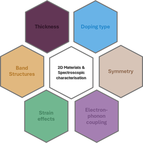
Figure 8. Characterisations of 2D materials with spectroscopy overview.
Raman spectroscopy provides valuable insights into the properties of 2D materials. By examining the shifts and intensity ratios of specific peaks, such as the G and 2D peaks, it reveals the number of layers in a material, like graphene. The D peak, on the other hand, can indicate defects and disorder in the material, with the intensity ratio of D to G (ID/IG) offering information on defect density and overall material quality. Additionally, Raman spectroscopy helps understand the phonon modes, which are important for exploring the material’s vibrational properties and how it interacts with its surroundings.
PL spectroscopy reveals details about the material’s bandgap, with the energy and intensity of the PL peaks indicating the presence of defects or impurities. PL is particularly useful for studying excitonic behaviour, especially in materials like monolayer semiconductors, where excitons (bound states of electrons and holes) play an important role. By analysing the PL spectra, researchers can gain insights into the material’s quality and its potential for applications in optoelectronics.
SHG provides valuable information about the symmetry and nonlinear optical properties of 2D materials. Since SHG is sensitive to the material’s symmetry, it can reveal whether a material lacks inversion symmetry, as seen in monolayer materials like MoS₂, which show a strong SHG response. The intensity of the SHG signal can also give insights into the alignment and orientation of the material. Additionally, SHG is used to probe the material’s nonlinear optical properties, which are essential for applications in photonics, sensing, and imaging.
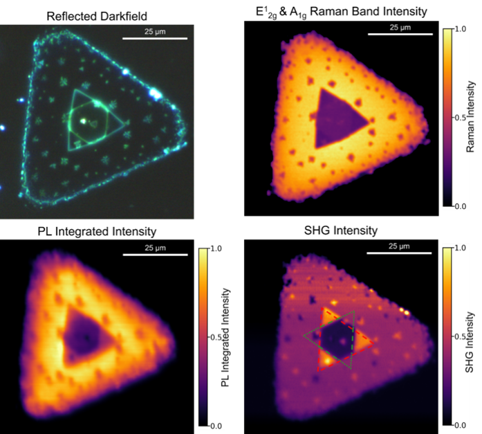
Figure 9. Multimodal analysis of a WSe2 crystal using Raman, PL and SHG.
In a nutshell:
Raman: “What atoms are here, how are they arranged, and are there any defects?”
PL: “How do electrons behave and interact with light, and what is the bandgap?”
SHG: “What is the precise structure and symmetry, and what are the nonlinear optical properties?”
2D Materials: A Glimpse into Tomorrow’s World
From the groundbreaking discovery of graphene to the exciting potential of TMDs, MXenes, phosphorene, and hBN, 2D materials are revolutionising science and technology. These atomically thin materials offer a unique combination of properties, opening doors to innovations in electronics, energy, medicine, and beyond.
While challenges remain in large-scale manufacturing and integration, the ongoing research and development in this field promise a future where 2D materials are at the heart of countless everyday devices, shaping a world that is faster, more efficient, and more sustainable. With powerful characterisation tools like those offered by Edinburgh Instruments, researchers are well-equipped to explore the full potential of these atomic wonders.