Skip to content
Skip to content
  • News
  • Events
  • eBooks
  • Blog
  • Careers
  • Contact
  • News
  • Events
  • eBooks
  • Blog
  • Careers
  • Contact
KNOWLEDGEBASE
  • About Us
  • Products

    Fluorescence Spectrometers

    • FLS1000 Photoluminescence Spectrometer
    • FS5 Spectrofluorometer
    • LifeSpec II Lifetime Spectrometer
    • Mini-tau Lifetime Spectrometer

    Raman Microscopes

    • RM5 Raman Microscope
    • RMS1000 Multimodal Confocal Microscope

    Transient Absorption

    • LP980 Transient Absorption Spectrometer

    FTIR Spectrometers

    • IR5 FTIR Spectrometer

    Lasers and LEDs

    • Pulsed Lasers
    • Gas Lasers
    • Customisation Options
    View All Products
  • Techniques
  • Applications
KNOWLEDGEBASE
Edit Content
  • About Us
  • Products
  • Techniques
  • Applications
  • Knowledgebase
  • eBooks
  • News
  • Events
  • Blog
  • Careers
  • Contact Us
  1. Home
  2. Blog Post
  3. Map of the Month – GaN Strain Imaging

BLOG

Map of the Month – GaN Strain Imaging

  • January 13, 2025

KEY POINTS

  • In semiconductors like gallium nitride (GaN), stress-induced deformation of the crystal lattice can occur, which influences the bandgap and charge carrier mobility.  
  • Manufacturers of GaN-based devices must monitor for strain because it can adversely affect performance.  
  • Raman microscopy can be used to generate strain images of GaN because an increase/decrease in the Raman modes of the material indicates compressive/tensile strain, respectively. 
Edit Content

Welcome to Edinburgh Instruments’ blog celebrating our work in Raman, Photoluminescence, and Fluorescence Lifetime Imaging. Every month, we aim to highlight our pick for Map of the Month to show how our Raman and fluorescence spectrometers can be used to reveal all the hidden secrets in your samples.  

January 2025 

To obtain high-quality optoelectronic devices containing GaN, manufacturers must ensure minimal mechanical and electrical heterogeneity caused by stress-induced crystalline deformations. These can cause changes in the bandgap and charge carrier mobility of the material and can significantly reduce the properties of the material.  


Non-destructive analytical techniques sensitive to these phenomena, of which Raman spectroscopy is an excellent example, are therefore essential to monitor GaN during manufacturing. As will be shown, it is sensitive to even the most subtle changes in the material and when coupled to a microscope, the spatial resolution of different stress and crystallinity states within the material is possible.   


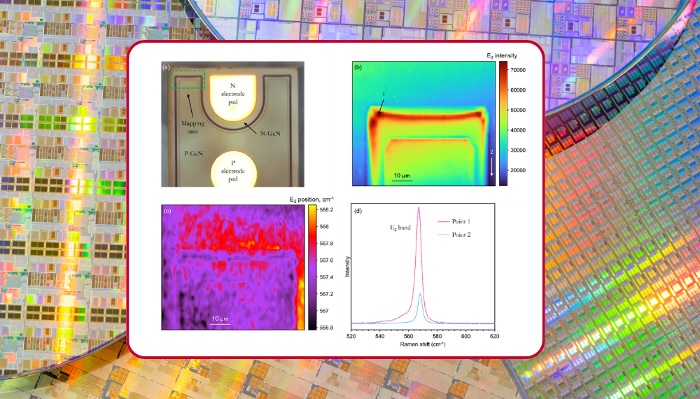
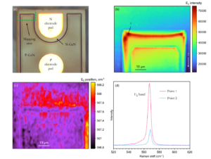
In our recent Application Note, we showed how the Edinburgh Instruments RMS1000 Confocal Microscope can be used to perform Raman and PL imaging on a GaN-based LED device, a picture of which is shown in panel (a) above. In this Map of the Month, we highlight the information provided about the LED by Raman imaging.  


An area of the GaN chip was imaged using spectral mapping with a 638 nm laser. To determine the distribution of GaN within this area, the intensity of the E2 (high) mode was imaged, Figure 4b. 


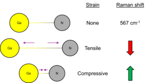
The position of the E2 (high) was imaged and is shown in panel (c). The Raman shift of this mode can be correlated with strain in GaN, with an increase in Raman shift relative to 567 cm-1 showing compressive strain and a decrease showing tensile strain, respectively. The image below shows how tensile and compressive strain affect bond lengths and atomic positions within a lattice. Raman microscopy can readily visualise strain on semiconductor materials such as GaN and silicon.  


In the image in panel (c), yellow and red regions indicate areas where the GaN is experiencing compressive strain, and the black regions represent areas of tensile strain. The spectra in panel (d) show the variation in intensity and peak position of the GaN E2 band across the images.  


Read our full Application Note to find out more about how Raman and PL microscopy were used to analyse this GaN-based LED.  

RELATED PRODUCTS

RMS1000

Multimodal Confocal Microscope

VIEW

RM5

Raman Microscope

VIEW

RESOURCES

Tags:
  • Map of the Month
Featured Product:

RMS1000 Raman Microscope

View more »
Suggested Reading:

Raman and Photoluminescence Characterisation of GaN

View more »

Raman Imaging of Strain in a Silicon Semiconductor Wafer

View more »
Share:
PrevPrevious
NextNext

Keep up to date with the latest from Edinburgh Instruments

Join our mailing list and keep up with our latest videos, app notes and more!

LOCATION:
  • Edinburgh Instruments Ltd.
    2 Bain Square, Kirkton Campus, Livingston, EH54 7DQ.
  • sales@edinst.com
  • +44 1506 425 300
ABOUT:
  • About Us
  • Techniques
  • Applications
  • Knowledgebase
  • About Us
  • Techniques
  • Applications
  • Knowledgebase
PRODUCTS:
  • Fluorescence Spectrometers
  • Raman Microscopes
  • UV-Vis Spectrophotometers
  • Transient Absorption
  • FTIR Spectrometers
  • Lasers and LEDs
  • Customisation Options
  • Software
  • Upgrades
  • All Products
  • Fluorescence Spectrometers
  • Raman Microscopes
  • UV-Vis Spectrophotometers
  • Transient Absorption
  • FTIR Spectrometers
  • Lasers and LEDs
  • Customisation Options
  • Software
  • Upgrades
  • All Products
LEGALS:
  • News
  • Events
  • Blog
  • Careers
  • Contact Us
  • Terms and Conditions
  • Privacy Policy
  • News
  • Events
  • Blog
  • Careers
  • Contact Us
  • Terms and Conditions
  • Privacy Policy
SOCIALS:
Youtube Linkedin X-twitter Facebook
©2024 Edinburgh Instruments. Registered in England and Wales No: 962331. VAT No: GB 271 7379 37
Manage Consent
To provide the best experiences, we use technologies like cookies to store and/or access device information. Consenting to these technologies will allow us to process data such as browsing behaviour or unique IDs on this site. Not consenting or withdrawing consent, may adversely affect certain features and functions.
Functional Always active
The technical storage or access is strictly necessary for the legitimate purpose of enabling the use of a specific service explicitly requested by the subscriber or user, or for the sole purpose of carrying out the transmission of a communication over an electronic communications network.
Preferences
The technical storage or access is necessary for the legitimate purpose of storing preferences that are not requested by the subscriber or user.
Statistics
The technical storage or access that is used exclusively for statistical purposes. The technical storage or access that is used exclusively for anonymous statistical purposes. Without a subpoena, voluntary compliance on the part of your Internet Service Provider, or additional records from a third party, information stored or retrieved for this purpose alone cannot usually be used to identify you.
Marketing
The technical storage or access is required to create user profiles to send advertising, or to track the user on a website or across several websites for similar marketing purposes.
Manage options Manage services Manage {vendor_count} vendors Read more about these purposes
View preferences
{title} {title} {title}