Skip to content
Skip to content
  • News
  • Events
  • eBooks
  • Blog
  • Careers
  • Contact
  • News
  • Events
  • eBooks
  • Blog
  • Careers
  • Contact
KNOWLEDGEBASE
  • About Us
  • Products

    Fluorescence Spectrometers

    • FLS1000 Photoluminescence Spectrometer
    • FS5 Spectrofluorometer
    • LifeSpec II Lifetime Spectrometer
    • Mini-tau Lifetime Spectrometer

    Raman Microscopes

    • RM5 Raman Microscope
    • RMS1000 Multimodal Confocal Microscope

    Transient Absorption

    • LP980 Transient Absorption Spectrometer

    FTIR Spectrometers

    • IR5 FTIR Spectrometer

    Lasers and LEDs

    • Pulsed Lasers
    • Gas Lasers
    • Customisation Options
    View All Products
  • Techniques
  • Applications
KNOWLEDGEBASE
Edit Content
  • About Us
  • Products
  • Techniques
  • Applications
  • Knowledgebase
  • eBooks
  • News
  • Events
  • Blog
  • Careers
  • Contact Us
  1. Home
  2. Blog Post
  3. Map of the Month – Imaging Tungsten Disulfide

BLOG

Map of the Month – Imaging Tungsten Disulfide

  • December 2, 2022
Edit Content

Welcome to Edinburgh Instruments monthly blog celebrating our work in Raman, Photoluminescence, and Fluorescence Lifetime Imaging. Every month we will highlight our pick for Map of the Month to show how our spectrometers can be used to reveal all the hidden secrets in your samples.

December

2D materials are an emerging class of thin-layer crystals of interest due to their unique optoelectronic properties. The first in this class to gain traction was graphene, now inorganic 2D materials called transition metal dichalcogenides (TMDs) are gaining popularity. The most commonly studied materials in this field are MoS­2, MoSe2, WS2, and WSe2. In bulk form these materials have an indirect band gap, however, when they are grown as monolayer and few-layer crystals, they become direct band gap semiconductors. This property in particular has prompted substantial research into their physical characteristics for optoelectronic devices.

Identifying the number of layers, strain, defects, and doping in 2D TMDs is critical for using these materials successfully. Raman and photoluminescence (PL) microscopy can provide highly detailed sample information in these crucial areas. A 532 nm excitation will provide both Raman and PL spectra from 2D TMDs and their bands can be analysed for complex sample evaluation.

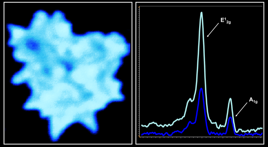
Figure 1: Raman intensity map (left) and representative spectra (right) from a WS2 crystal at areas of different layer thickness.

WS2 is an interesting 2D TMD not only for the properties it shares with other materials in this category, it also offers additional advantages such as strong thermal stability and ambipolar field-modulation behaviour. The main two bands of interest in the Raman spectrum are the E12g and A1g modes representative of in-plane and out-of-plane vibrations respectively. As the number of layers increases so too does the Raman intensity of these bands, therefore, imaging a WS2 crystal reveals areas of higher intensity that in turn represent increased layer thickness, Figure 1.

Figure 2: PL intensity map from a WS2 crystal.

PL mapping is particularly sensitive to the number of layers as well. In fact, the PL peak only appears as we obtain thin layers of WS2, and bulk material produces no PL. These crystals are particularly large and areas of the crystal produce little to no PL indicating a thick layer of WS2 where it is starting to lose its direct band gap, Figure 2. When looking at a sample which presents areas of monolayer and multilayer WS­2, the PL intensity can easily be used for layer evaluation. Figure 3 details such a case, the reflected brightfield image (Figure 3(a)) shows a triangle which appears to have multiple layers of WS2 in the centre. Plotting the PL intensity map reveals no PL response in the centre meaning there is a thicker layer of WS2 present in the centre, Figure 3(b).

Figure 3: Analysis of a WS2 crystal – (a) brightfield reflected image (b) PL intensity map (c-d) PL spectra from an area of monolayer and multilayer WS2, highlighting intensity and peak position respectively.

Figure 3(b) also shows a variation in PL intensity on the outer triangle of the sample, this is representative of monolayer and multilayer WS2. The difference in intensity between areas of monolayer and areas of multilayer WS2 has been plotted in Figure 3(c) to highlight the significant difference in intensity between the two areas. A shift in PL peak position is also seen, Figure 3(d), as the sample becomes monolayer the peak is red-shifted in comparison to areas of multilayer WS2 (note the spectra have been normalised for simple comparison).

Raman Microscopes from Edinburgh Instruments

To find out more about how our Raman Microscopes can benefit your research, contact our sales team today who will be happy to help you.

Keep in Touch

If you have enjoyed reading this application note, why not sign-up to our monthly eNewsletter via the button below or follow us on your favourite social media channel in the footer below to keep up to date with our latest news and research.

RELATED PRODUCTS

RESOURCES

Tags:
  • Map of the Month
  • 2D Materials
  • RMS1000
  • Photoluminescence
  • Raman
Application Notes:
Featured Product:

RMS1000 Raman Microscope

View more »

RM5 Raman Microscope

View more »
Suggested Reading:

Ramacle® Software Highlight: FastMAP®

View more »
Share:
PrevPrevious
NextNext

Keep up to date with the latest from Edinburgh Instruments

Join our mailing list and keep up with our latest videos, app notes and more!

LOCATION:
  • Edinburgh Instruments Ltd.
    2 Bain Square, Kirkton Campus, Livingston, EH54 7DQ.
  • sales@edinst.com
  • +44 1506 425 300
ABOUT:
  • About Us
  • Techniques
  • Applications
  • Knowledgebase
  • About Us
  • Techniques
  • Applications
  • Knowledgebase
PRODUCTS:
  • Fluorescence Spectrometers
  • Raman Microscopes
  • UV-Vis Spectrophotometers
  • Transient Absorption
  • FTIR Spectrometers
  • Lasers and LEDs
  • Customisation Options
  • Software
  • Upgrades
  • All Products
  • Fluorescence Spectrometers
  • Raman Microscopes
  • UV-Vis Spectrophotometers
  • Transient Absorption
  • FTIR Spectrometers
  • Lasers and LEDs
  • Customisation Options
  • Software
  • Upgrades
  • All Products
LEGALS:
  • News
  • Events
  • Blog
  • Careers
  • Contact Us
  • Terms and Conditions
  • Privacy Policy
  • News
  • Events
  • Blog
  • Careers
  • Contact Us
  • Terms and Conditions
  • Privacy Policy
SOCIALS:
Youtube Linkedin X-twitter Facebook
©2024 Edinburgh Instruments. Registered in England and Wales No: 962331. VAT No: GB 271 7379 37
Manage Consent
To provide the best experiences, we use technologies like cookies to store and/or access device information. Consenting to these technologies will allow us to process data such as browsing behaviour or unique IDs on this site. Not consenting or withdrawing consent, may adversely affect certain features and functions.
Functional Always active
The technical storage or access is strictly necessary for the legitimate purpose of enabling the use of a specific service explicitly requested by the subscriber or user, or for the sole purpose of carrying out the transmission of a communication over an electronic communications network.
Preferences
The technical storage or access is necessary for the legitimate purpose of storing preferences that are not requested by the subscriber or user.
Statistics
The technical storage or access that is used exclusively for statistical purposes. The technical storage or access that is used exclusively for anonymous statistical purposes. Without a subpoena, voluntary compliance on the part of your Internet Service Provider, or additional records from a third party, information stored or retrieved for this purpose alone cannot usually be used to identify you.
Marketing
The technical storage or access is required to create user profiles to send advertising, or to track the user on a website or across several websites for similar marketing purposes.
Manage options Manage services Manage {vendor_count} vendors Read more about these purposes
View preferences
{title} {title} {title}