Skip to content
  • News
  • Events
  • eBooks
  • Blog
  • Careers
  • Contact
  • News
  • Events
  • eBooks
  • Blog
  • Careers
  • Contact
KNOWLEDGEBASE
  • About Us
  • Products

    Fluorescence Spectrometers:

    • FLS1000 Photoluminescence Spectrometer
    • FS5 Spectrofluorometer
    • LifeSpec II Lifetime Spectrometer
    • Mini-tau Lifetime Spectrometer

    Raman Microscopes:

    • RM5 Raman Microscope
    • RMS1000 Multimodal Confocal Microscope

    Transient Absorption:

    • LP980 Transient Absorption Spectrometer

    FTIR Spectrometers:

    • IR5 FTIR Spectrometer

    Lasers and LEDs:

    • Pulsed Lasers
    • Gas Lasers

    Options:

    • Upgrades
    • Customisation
    View All Products
  • Techniques
  • Applications
KNOWLEDGEBASE
  • About Edinburgh Instruments
  • Products
  • Techniques
  • Applications Old
  • Knowledgebase
  • eBooks
  • News
  • Events
  • Blog
  • Careers
  • Contact Us

RESOURCES

Semiconductors: Advanced Spectroscopic Characterisation

  • September 25, 2025

KEY POINTS

  • Raman spectroscopy and photoluminescence (PL) provide complementary insights into the structure and optoelectronic performance of semiconductors.
  • Multimodal microscopy can correlate defects, strain, crystallinity and radiative efficiency at the microscale.
  • 3D Raman imaging can reveal the chemical identity and morphology of subsurface defects in semiconductor materials.
  • Wafer-scale Raman and PL mapping extends spectroscopic characterisation from individual devices to semiconductor quality control and uniformity testing.

Semiconductor performance is closely linked to material structure. Strain, defects, doping and variations in crystallinity can all influence how a device behaves, making techniques that connect structure with optical performance particularly valuable.

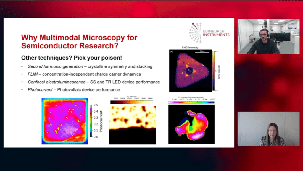
In this Edinburgh Instruments webinar, Dr Matthew Berry and Angela Flack explore advanced Raman spectroscopy, PL and multimodal microscopy through semiconductor case studies spanning silicon, silicon carbide, gallium nitride LEDs and wafer-scale analysis.


Combining Raman and Photoluminescence

Raman spectroscopy offers high chemical and structural specificity, enabling changes in crystal structure, strain, crystallinity and film thickness to be investigated. PL provides complementary information on semiconductor band gaps and radiative efficiency. Bringing both techniques together enables structural and optoelectronic information to be collected from the same region of a sample, providing a more complete picture of material performance.

In silicon, simultaneous Raman and PL imaging was combined with principal component analysis (PCA) to identify a defect exhibiting both a shift in the Raman phonon mode and reduced PL. This correlated structural variation, potentially associated with strain or doping, with a reduction in radiative efficiency.


Revealing Semiconductor Defects in 3D

For silicon carbide, confocal Raman microscopy takes defect characterisation into three dimensions. By rejecting out-of-focus light and optically sectioning the sample, Raman maps can reveal both the chemical composition and spatial extent of features beneath the surface.

In the webinar case study, Raman spectroscopy differentiated the expected 4H-SiC from a 6H-SiC polytype inclusion. 3D Raman imaging showed that the inclusion formed a pipe-like feature extending more than 3 µm into the wafer, demonstrating how Raman microscopy can provide both chemical and morphological information on semiconductor defects.


Connecting Strain with LED Performance

Multimodal spectroscopy can also directly correlate material structure with device performance. In a gallium nitride LED, Raman mapping tracked variations in the strain-sensitive E2 high phonon mode, while PL mapping provided a corresponding view of optical performance.

Overlaying the datasets revealed that regions of higher strain corresponded with lower PL intensity. Raman therefore identified where the crystal lattice was distorted, while PL showed how efficiently those regions emitted light, establishing a direct structure-performance relationship across the device.


From Microscopy to Full-Wafer Mapping

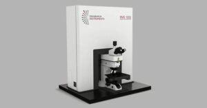
The same Raman and PL approaches can be scaled from individual semiconductor structures to complete wafers. With the Edinburgh Instruments RMS1000 Multimodal Confocal Microscope, wafer mapping can automate spectral acquisition across the surface and assess parameters such as Raman or PL peak position, intensity and linewidth against user-defined tolerances.

This provides a route to assessing semiconductor uniformity and identifying regions that fall outside required specifications, extending multimodal spectroscopy from research and development towards wafer-level quality control.


Watch the Semiconductors Webinar

Watch the full webinar to see Dr Matthew Berry and Angela Flack explain how Raman spectroscopy, PL, 3D Raman imaging, and wafer mapping can uncover defects, investigate strain and connect semiconductor structure with optoelectronic performance, from individual microscopic features through to entire wafers.
Read More Read Less

RELATED PRODUCTS

RMS1000

Multimodal Confocal Microscope

VIEW

Contact our expert team today to find out more about how our products can improve your research

Contact Us
PrevPrevious
NextNext
Previous Photo- and Radio-Luminescence of Copper Cluster Scintillators Next Fluorescent Sensors for Selective and Sensitive Morphine Detection

RESOURCES

Semiconductors Webinar Featured Image
Tags:
  • Webinars
  • Semiconductors
  • RMS1000
  • Photoluminescence
  • Raman
Featured Product:

RMS1000 Raman Microscope

View more »
Suggested Reading:

Raman Thermometry of a Silicon Semiconductor Chip

View more »

Raman Spectroscopy of Silicon Carbide Semiconductor Wafers

View more »
Share:

Keep up to date with the latest from Edinburgh Instruments

Join our mailing list and keep up with our latest videos, app notes and more!

LOCATION:
  • Edinburgh Instruments Ltd.
    2 Bain Square, Kirkton Campus, Livingston, EH54 7DQ
  • sales@edinst.com
  • +44 1506 425 300
ABOUT:
  • About Edinburgh Instruments
  • Techniques
  • Applications
  • Knowledgebase
  • About Edinburgh Instruments
  • Techniques
  • Applications
  • Knowledgebase
PRODUCTS:
  • Fluorescence Spectrometers
  • Raman Microscopes
  • UV-Vis Spectrophotometers
  • Transient Absorption
  • FTIR Spectrometers
  • Lasers and LEDs
  • Customisation Options
  • Software
  • Upgrades
  • All Products
  • Fluorescence Spectrometers
  • Raman Microscopes
  • UV-Vis Spectrophotometers
  • Transient Absorption
  • FTIR Spectrometers
  • Lasers and LEDs
  • Customisation Options
  • Software
  • Upgrades
  • All Products
LEGALS:
  • News
  • Events
  • Blog
  • Careers
  • Distribution & Agents
  • Contact Us
  • Terms and Conditions
  • Privacy Policy
  • Coordinated Vulnerability Disclosure Policy
  • News
  • Events
  • Blog
  • Careers
  • Distribution & Agents
  • Contact Us
  • Terms and Conditions
  • Privacy Policy
  • Coordinated Vulnerability Disclosure Policy
SOCIALS:
Youtube Linkedin X-twitter Facebook
©2026 Edinburgh Instruments. Registered in England and Wales No: 962331. VAT No: GB 271 7379 37
Manage Consent
To provide the best experiences, we use technologies like cookies to store and/or access device information. Consenting to these technologies will allow us to process data such as browsing behaviour or unique IDs on this site. Not consenting or withdrawing consent, may adversely affect certain features and functions.
Functional Always active
The technical storage or access is strictly necessary for the legitimate purpose of enabling the use of a specific service explicitly requested by the subscriber or user, or for the sole purpose of carrying out the transmission of a communication over an electronic communications network.
Preferences
The technical storage or access is necessary for the legitimate purpose of storing preferences that are not requested by the subscriber or user.
Statistics
The technical storage or access that is used exclusively for statistical purposes. The technical storage or access that is used exclusively for anonymous statistical purposes. Without a subpoena, voluntary compliance on the part of your Internet Service Provider, or additional records from a third party, information stored or retrieved for this purpose alone cannot usually be used to identify you.
Marketing
The technical storage or access is required to create user profiles to send advertising, or to track the user on a website or across several websites for similar marketing purposes.
  • Manage options
  • Manage services
  • Manage {vendor_count} vendors
  • Read more about these purposes
View preferences
  • {title}
  • {title}
  • {title}