Understanding how structural defects influence the optoelectronic performance of silicon semiconductor wafers is crucial for optimising device efficiency and reliability. Traditional univariate approaches, such as tracking Raman peak shifts to assess strain or monitoring photoluminescence (PL) intensity to evaluate non-radiative recombination in semiconductors, are powerful but inherently limited. They require manual feature selection and assume independent behaviour of each parameter. This means potentially valuable correlations between strain, crystallinity, and emission efficiency may be missed, or discovered only through time-consuming manual cross-analysis.
Multivariate analysis techniques, such as Principal Component Analysis (PCA) and K-means clustering (KMC), offer a powerful alternative. Rather than requiring the user to choose which spectral features to examine, these methods analyse the whole dataset and automatically extract the most important patterns, often revealing trends that might not have been anticipated.
These methods not only reduce the complexity of high-dimensional Raman and PL imaging data, but also reveal hidden correlations between structural changes and their impact on radiative efficiency. By applying multivariate techniques, we gain a comprehensive understanding of how strain, crystallinity, and defect distributions collectively affect silicon’s electronic properties and PL behaviour. Table 1 highlights several advantages that multivariate analysis has over univariate analysis.
Table 1. Why use multivariate analysis?
| Feature | Univariate | Multivariate |
| Feature selection | Manual and prior-knowledge-based | Automatic, data-driven |
| Correlation detection | Manual comparison | Captured automatically |
| Noise handling | Limited | Low-variance noise filtered |
| Result interpretation | Potential for subjectivity | Mathematical basis |
| Scalability | Time-consuming | Highly scalable |
This Application Note demonstrates the use of simultaneous Raman and PL imaging combined with multivariate analysis to image and interpret the complex spatial variations in silicon wafers. Through this integrated approach, we connect structural heterogeneities directly to changes in radiative emission, enabling more effective defect characterisation and process monitoring.
The silicon wafer analysed in this study was sourced from PI-KEM and examined using an Edinburgh Instruments RM5 Confocal Raman Microscope equipped with an 830 nm laser, Figure 1. The system was operated in FastMAP® mode, enabling rapid acquisition of high-resolution spectral images. Raman and PL signals were collected simultaneously using a front-illuminated-CCD detector capable of detecting NIR emissions.
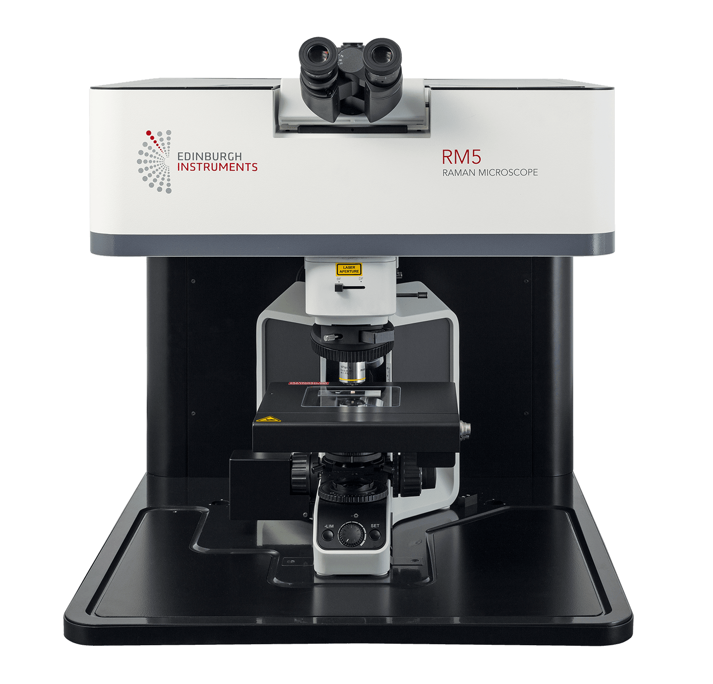
Figure 1. An Edinburgh Instruments RM5 Confocal Raman Microscope.
Multivariate techniques were employed to handle the high-dimensional data from the Raman-PL images, consisting of thousands of spectra across the wafer. PCA was applied to reduce data dimensionality and extract the most significant spectral variations linked to structural and optical properties.
Additionally, KMC was used to classify regions with similar spectral characteristics, providing clear segmentation of defect sites and homogeneous areas. Data processing and visualisation were performed in the Ramacle Python-IDE.
The region analysed on the wafer is shown in Figure 2a. An 830 nm laser was used with a 600 gr/mm grating, which meant that the dominant phonon mode at 520 cm-1 could be detected along with the broad PL band present in the Raman spectrum at ca. 1900 cm-1, as seen in Figure 2b.
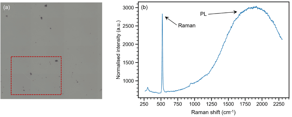
Figure 2. Initial microscopic and spectroscopic interrogation of the silicon wafer. (a) White light image of the area analysed on the wafer. (b) A spectrum recorded at 830 nm showing Raman and PL bands from the silicon.
The silicon wafer dataset contains interrelated information on strain, crystallinity, and emission efficiency that univariate analyses often overlook; multivariate techniques, on the other hand, automatically extract these relationships, enabling rapid and objective interpretation of large datasets.1
The first multivariate technique used was PCA, a widely used dimensionality reduction technique that simplifies complex datasets while preserving the most important patterns.2 To better understand what this means, consider the spectral image of the silicon wafer that we want to analyse. The image was 236 pixels by 230 pixels, totalling 54,280 pixels, each containing a spectrum with 1650 datapoints (or dimensions). This is a huge amount of data, and it is computationally prohibitive. PCA addresses this issue by performing a linear transformation that outputs a small number of new variables, designed to maximise the variance from the original dataset, called principal components (PCs).
The Python script used in this Application Note outputs the five PCs that explain the dominant Raman and PL modes of variation within the original image, along with loading vectors that show the bands contributing to the spectral variance. The 1650 dimensions of the previous dataset are reduced to five, and the irrelevant information from the original dataset is filtered out as noise. Each pixel within the image will therefore have five PC scores (PC1-5), which can be spatially mapped to reveal the most relevant spectral changes within the dataset.
In the silicon wafer image dataset, PC1 and PC3 showed large variations in the PL and Raman bands, respectively. Score maps and loading vector plots for both PCs are shown in Figure 3. A defect, shown in the blue ellipsoid in Figure 3a, was of particular interest for this analysis because of the drastic difference in spectral response compared to the rest of the wafer. This region corresponds to a thin streak visible in the white-light image of the wafer, as shown in the red box in Figure 2a.
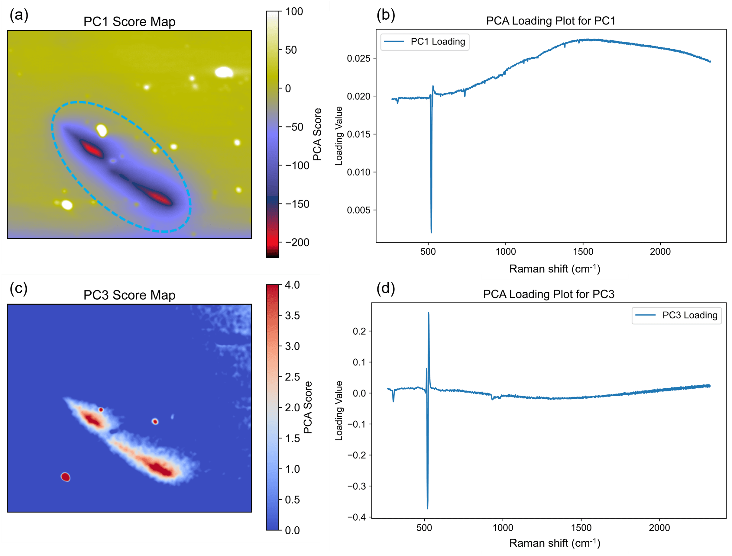
Figure 3. PCA imaging of the silicon wafer. (a) Score map and (b) loading vector plot for PC1. (c) Score map and (d) loading vector plot for PC3.
Figures 3a and 3b show the score map and loading plot, respectively, for PC1. The loading plot shows that PC1 represents the contrast between the silicon Raman and PL bands, because the Raman band at 520 cm-1 is strongly negative and the PL band at 1900 cm-1 is strongly positive. Therefore, positive scoring in PC1 corresponds to a dominant PL band, and negative scoring corresponds to dampened PL with respect to the Raman band. The defect in the PC1 map is scored negatively (purple and red), suggesting that the PL in this region is weaker relative to the Raman scattering, compared to other regions on the wafer.
The score map and loading point for PC3 are shown in Figures 3c and 3d, respectively. The loading plot shows that PC3 represents changes only in the Raman signature detected from the silicon, with almost no contributions from the PL band. There are large negative bands and large positive bands both in the vicinity of 520 cm-1, which indicates changes in the peak position and/or shape of the Raman band. This PC, therefore, indicates that PL is diminished in the defect, potentially due to a Raman-shift changing phenomenon such as strain.
Overall, PCA indicates that, in the highlighted defect on the silicon wafer, changes in the vibrational properties of the material correlate with a decrease in radiative emission.
While this structure-performance relationship could be identified by separately mapping and then comparing the Raman peak position and PL intensity, the multivariate analysis reveals these correlations directly and objectively, without requiring prior knowledge of which spectral features to examine.
KMC was also performed on the dataset to more clearly visualise the spatial distribution of distinct spectral signatures across the silicon wafer. K-means is an unsupervised learning method that partitions datasets into ‘k’ clusters based on their similarity.3
In this Application Note, it was used to group image pixels with similar Raman and PL spectral signatures into distinct spatial regions. It works by assigning pixels to clusters, minimising the sum of squares within each cluster, and calculating the mean spectrum for each cluster. In the Python script used, the 54,280 spectra making up the silicon wafer image were divided among ten clusters. Each cluster was imaged discretely to visualise the heterogeneity of the wafer in a way that may not have been immediately apparent in the continuous colourmaps used in PCA imaging. The KMC image of the wafer is shown in Figure 4a.
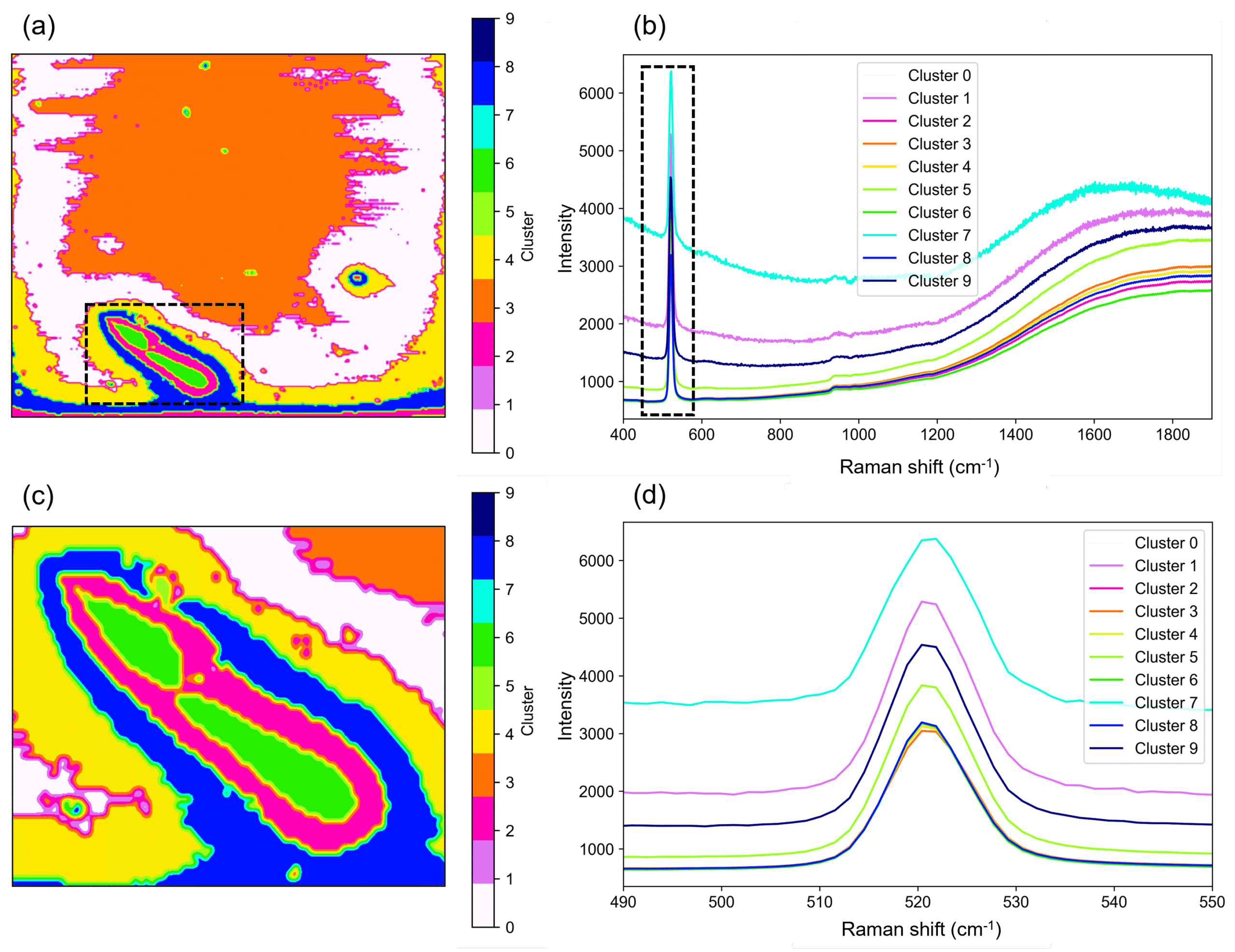
Figure 4. KMC imaging of the silicon wafer. (a) KMC image. (b) Mean spectra for each cluster. (c) Magnified view of the defect structure. (d) Magnified view of the Raman peak region.
The cluster image in Figure 4a clearly delineates the defect structure identified earlier, with significant inter-defect variation highlighted by Cluster 6 (green) and Cluster 3 (pink). The mean spectra from each cluster are highlighted in Figure 4b. Magnified views of the defect in the cluster image, and mean spectra focused on the Raman band alone, are shown in Figures 4c and 4d, respectively.
The mean spectrum from the green structure in the centre of the defect has a lower Raman shift compared to the surrounding pink structure, by about 2 cm-1. This analysis shows, therefore, that there is likely tensile strain in the silicon within the defect. Similarly to PC1, the PL in the green cluster is lower than the outside defect and the rest of the wafer. The consistent reduction in PL with tensile strain provides a clear correlation between structure and optoelectronic performance.
This Application Note highlights the value of multivariate techniques, specifically PCA and KMC, for analysing complex Raman and PL images of silicon wafers. These methods enable efficient dimensionality reduction and pattern recognition, revealing subtle variations in strain and emission properties that traditional univariate analysis would miss.
Together, these tools offer a fast, reliable approach for interpreting high-dimensional Raman and PL images. Their integration into Raman microscopy workflows enhances material characterisation and supports a deeper understanding of structure-property relationships in semiconductors. This approach can accelerate wafer quality control, streamline defect identification, and provide faster feedback during semiconductor manufacturing.