Welcome to Edinburgh Instruments’ blog, celebrating our work in Raman, Photoluminescence, and Fluorescence Lifetime Imaging. Every month, we aim to highlight our pick for Map of the Month to show how our Raman and fluorescence spectrometers can be used to reveal all the hidden secrets in your samples.
Silicon carbide (SiC) is a semiconductor increasingly employed in high-power electronics, such as inverters for EVs and solar grids.
Its superior material properties compared to silicon include a wider band gap (higher voltage/frequency, efficiency), higher thermal conductivity (better heat dissipation), chemical inertness (corrosion/oxidation resistance), and greater radiation hardness.
These attributes make SiC advantageous in applications prioritizing efficiency, size, and thermal management. Achieving optimal performance necessitates precise control of SiC crystal structure, quality, dopant concentration, and defect density during manufacturing, as these parameters critically affect material properties.
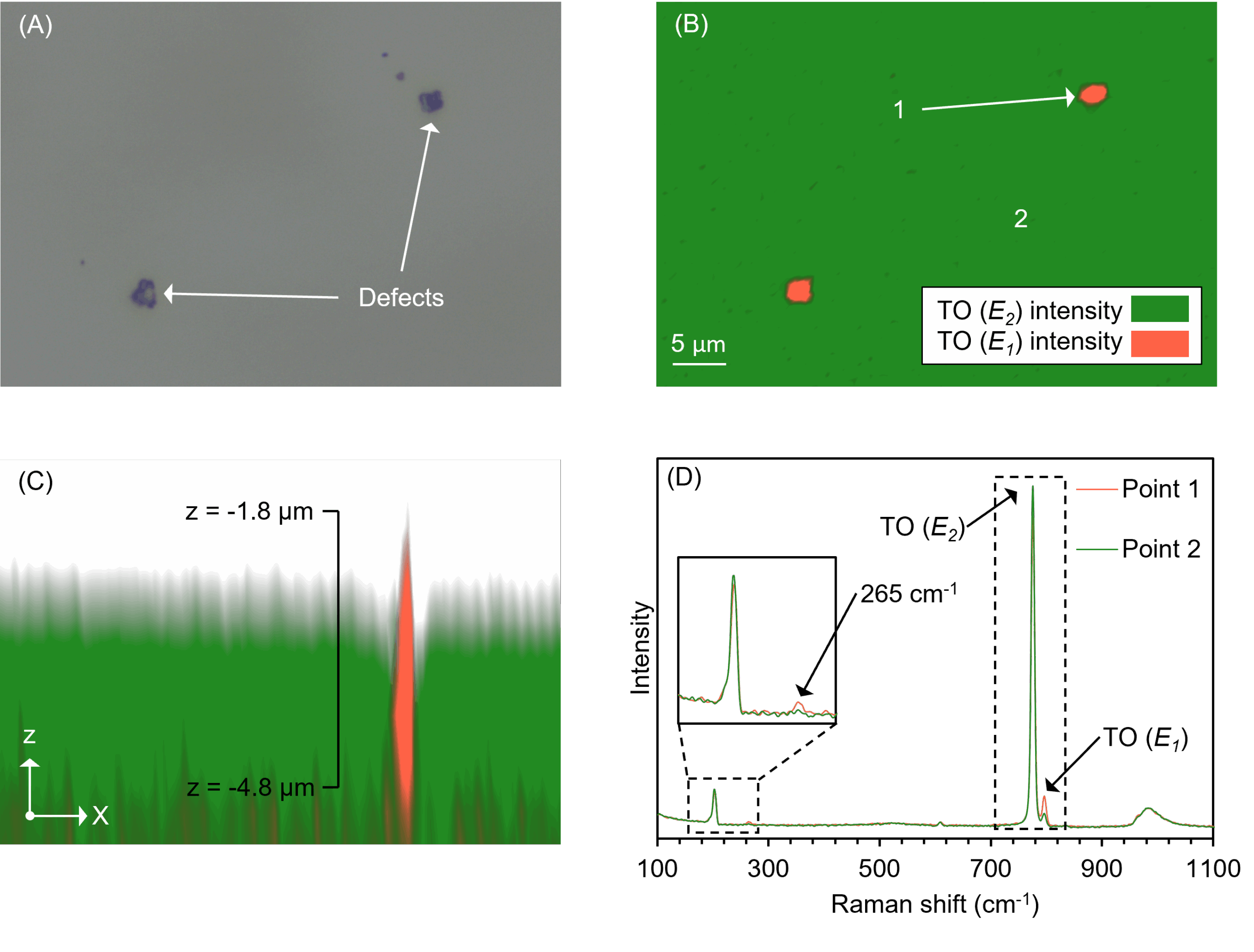
In this Map of the Month, we highlight our recent Application Note on the Raman imaging of SiC. In the image above, we use 3D Raman imaging to determine the morphological and chemical characteristics of crystalline defects in a SiC wafer. We were able to determine the size of the inclusions, how far they were embedded into the wafer, and their nature. Through analysis of the defect Raman spectra, we found that they were polytype inclusions; 6H-SiC in the 4H-SiC wafer.
We didn’t stop there in our Application Note. Give it a read to find out more about how Raman microscopy can be applied to the analysis of SiC.