Welcome to Edinburgh Instruments’ blog celebrating our work in Raman, Photoluminescence, and Fluorescence Lifetime Imaging. Every month, we aim to highlight our pick for Map of the Month to show how our Raman and fluorescence spectrometers can be used to reveal all the hidden secrets in your samples.

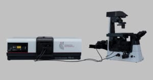
OLEDs light up our lives. They have rapidly become the technology of choice for full-colour display panels. They are responsible for the sharp, bright images we see on the very best televisions and high-end smartphones. Before they make their way into mass production, researchers need to make sure that any novel OLED materials meet the high-performance demands of the devices for which they are intended. This involves testing them for colour purity and flux distribution when electroluminescent under working conditions. We recently tested an OLED in the lab using the Edinburgh Instruments RMS1000 and found it great for providing highly detailed spatial mapping data on these properties.
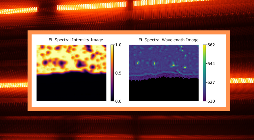
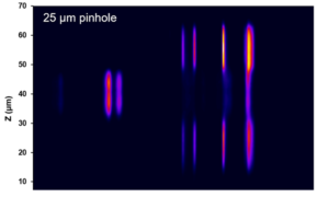
How did we do it? To allow the OLED to emit EL under the microscope, as shown in panels (a) and (b) above, we placed it in an electrical probe stage (LINKAM HFS350EV-PB4) and connected two tungsten probes to the electrodes intersecting on the OLED pixel of interest. We connected this stage to a Keithley 2450 Source Measurement Unit (SMU) to apply a bias to the OLED, and then we could detect the EL emissions on a CCD detector. We had to contend with the fact that there was no laser involved to provide spatial resolution. In standard photoluminescence (PL) or Raman measurements through a microscope, spatial resolution is predominantly determined by the laser spot size because only one small part of the sample is excited at a time. In contrast, here, the whole sample was emitting simultaneously. To get around this, we used the confocal pinhole on the RMS1000 to provide the spatial resolution by reducing the pinhole diameter to the smallest available setting of 25 μm.
So, what did the EL mapping tell us? The EL intensity image in (c) confirms what we see in the white light image in (b): less-emissive defects across the OLED device create a non-uniform luminosity distribution. This is undesirable for display technologies because it would mean that some areas would look brighter than others. We can determine the colour uniformity of the device by mapping the wavelength of the EL emissions across the map, shown in (d). This gives us even more detail about the OLED and shows us that the non-emissive defects are low-intensity redshifted EL bands. Therefore, the colour distribution across the OLED is also non-uniform. This could also cause visual issues if the OLED were installed on a display screen.
We hope you have learned more about display technology in this blog, but it is only the tip of the iceberg of our OLED research. Read our Application Note to learn more about how we used the RMS1000 to study an OLED’s spectral and time-resolved PL and EL.