Skip to content
  • News
  • Events
  • eBooks
  • Blog
  • Careers
  • Contact
  • News
  • Events
  • eBooks
  • Blog
  • Careers
  • Contact
KNOWLEDGEBASE
  • About Us
  • Products

    Fluorescence Spectrometers

    • FLS1000 Photoluminescence Spectrometer
    • FS5 Spectrofluorometer
    • LifeSpec II Lifetime Spectrometer
    • Mini-tau Lifetime Spectrometer

    Raman Microscopes

    • RM5 Raman Microscope
    • RMS1000 Multimodal Confocal Microscope

    Transient Absorption

    • LP980 Transient Absorption Spectrometer

    FTIR Spectrometers

    • IR5 FTIR Spectrometer

    Lasers and LEDs

    • Pulsed Lasers
    • Gas Lasers
    • Customisation Options
    View All Products
  • Techniques
  • Applications
KNOWLEDGEBASE
Edit Content
  • About Edinburgh Instruments
  • Products
  • Techniques
  • Applications
  • Knowledgebase
  • eBooks
  • News
  • Events
  • Blog
  • Careers
  • Contact Us

RESOURCES

FLIM Analysis of Light Emitting Diodes (LEDs): Mapping Defect-Induced Lifetime Variation in III/V Semiconductors

  • October 27, 2025

KEY POINTS

  • FLIM Microscopy provides spatially resolved mapping of photoluminescence lifetime in LED structures.
  • Lifetime variations reveal the presence of defects related to sidewall damage that impact recombination efficiency and consequently LED performance.
  • The MicroPL allows easy FLIM measurements and enables high-resolution mapping of III/V semiconductor LED chips.
Edit Content

Studying III/V Semiconductors with FLIM

Fluorescence Lifetime Imaging Microscopy (FLIM) is a technique used for characterising the photoluminescent (PL) properties of materials used in LEDs.1 By mapping PL lifetimes across a sample, FLIM provides insight into excited-state dynamics and local environments. This information is essential for understanding and improving LED efficiency and stability. 

Defects in III–V semiconductors significantly hinder LED performance by reducing radiative recombination efficiency. FLIM enables direct visualisation of these effects, guiding strategies to mitigate defect-related losses. 

III–V semiconductors such as AlInGaP and GaAs alloys are particularly attractive for LEDs due to their tuneable direct bandgaps (Figure 1). These materials enable emission across the visible spectrum while offering superior thermal stability and high device efficiency compared to II–VI or indirect-bandgap semiconductors such as silicon or silicon carbide. AlInGaP/GaAs LED chips, for example, are widely used for high-brightness red, orange, and yellow light emission.  

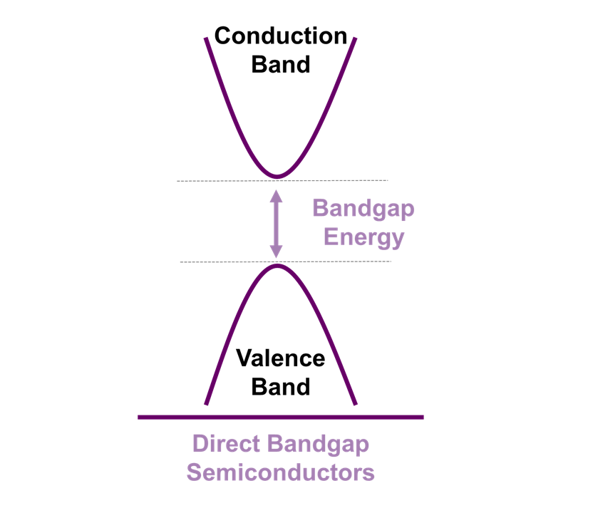
Figure 1. Direct bandgap of III/V-semiconductors illustrating the tuneability of emission wavelength in LED materials. 


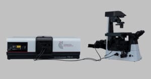
To fully exploit the potential of these high-performance materials, advanced characterisation tools are required. In this Application Note, we demonstrate how FLIM can be performed using the Edinburgh Instruments MicroPL upgrade, which can be coupled to the FS5 or FLS1000 PL spectrometers (Figure 2). The technique is used to study the emission properties of LEDs and can help in optimising chip design and understanding factors that limit performance. 

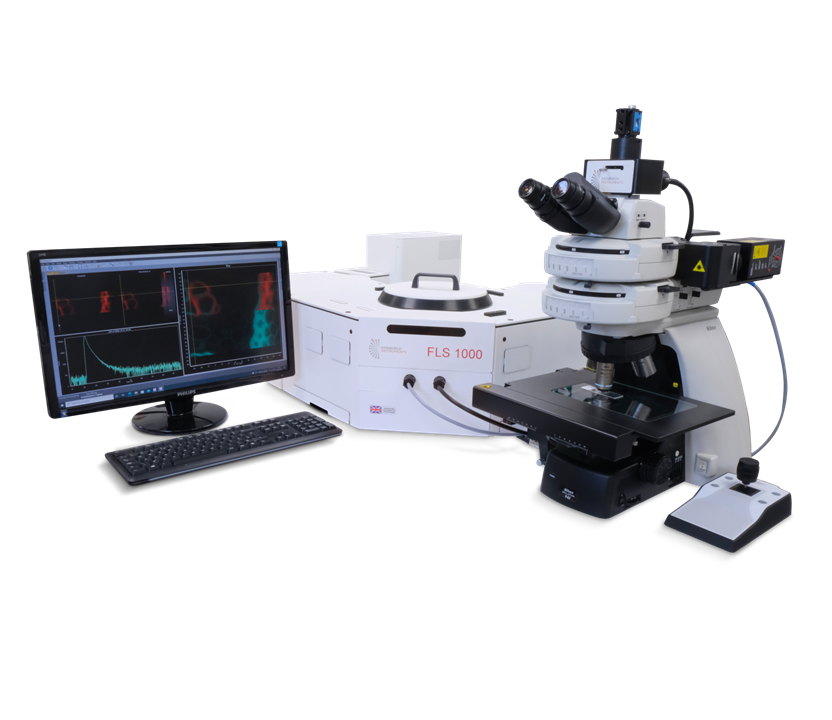
Figure 2. MicroPL coupled to an FLS1000 PL Spectrometer for FLIM mapping. 


Materials and Methods

AlInGaP/GaAs visible LED chips were investigated to study the PL properties of the epitaxial AlInGaP layer (Figure 3). The device under study was an orange LED emitting at 610 nm.  

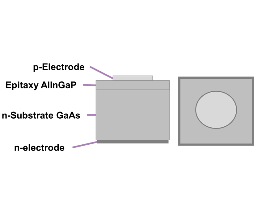
Figure 3. Structure of AlInGaP/GaAs LED Chip. 


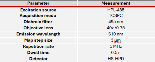
FLIM mapping was performed using the MicroPL upgrade with an FLS1000 spectrometer equipped with a 485 nm pulsed diode laser excitation source and high-speed hybrid photodetector (HS-HPD). PL lifetime measurements were collected using Time-Correlated Single Photon Counting (TCSPC). Full experimental parameters are shown in Table 1. 


Table1. Experimental parameters of FLIM mapping  

FLIM Mapping of LED Chip

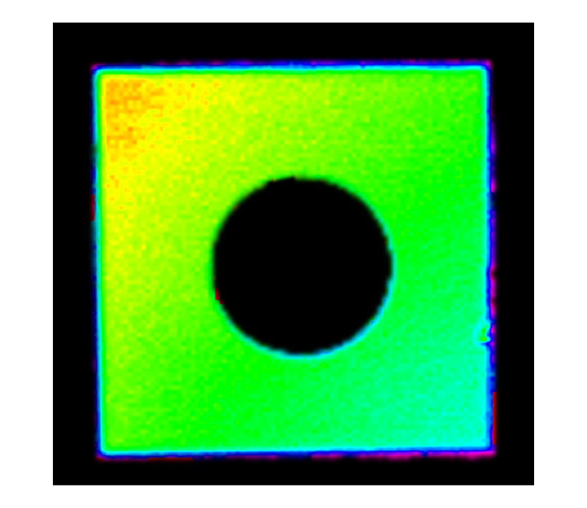
FLIM mapping of the LED chip surface, including the p-electrode and epitaxial AlInGaP layer, revealed spatial variations in lifetime (Figure 4). The results showed that the AlInGaP layer had an average lifetime of around 5.5 ns. It was observed that the lifetime decreased at the edges of the LED chip to around 2.5 ns. In addition, no PL signal was observed at the p-electrode on the chip, which is expected as the electrode material absorbs the excitation and PL light, preventing measurement of the underlying active layer. 


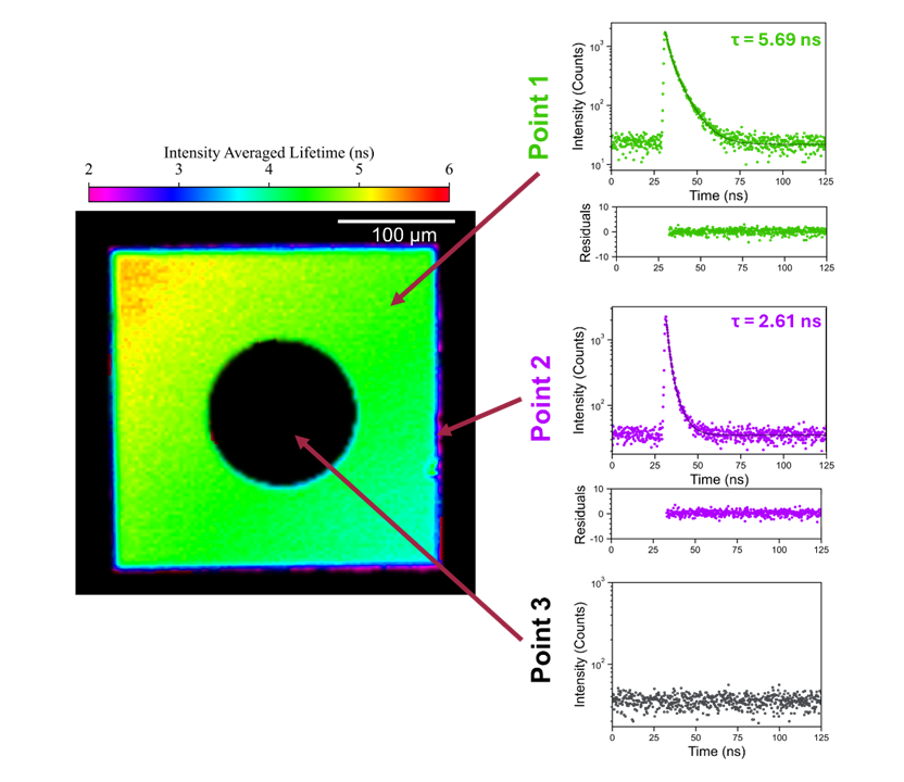
Figure 4. FLIM map of AlInGaP/GaAs LED chip showing variation in lifetime across the chip. Inset show PL lifetime at three distinct points of chip – Point 1: Epitaxy AlInGaP, Point 2: Edge of LED and Point 3: p-electrode. 


The reduced lifetime at the chip edge is attributed to the sidewall effect, which refers to the performance degradation caused by plasma damage to the LED’s sidewall during the fabrication process.2 These sidewall defects significantly influence device performance, affecting carrier dynamics, light extraction efficiency, and epitaxial layer quality. Optimising sidewall properties, such as angle, smoothness, and etch quality, is therefore critical for achieving high-performance LEDs. 


Conclusion

Using FLIM with the MicroPL upgrade for the FLS1000, we mapped the radiative recombination dynamics in AlInGaP/GaAs LEDs. This spatially resolved analysis revealed a significantly reduced carrier lifetime at the chip edges, directly correlating with the sidewall effect. These specific insights derived from FLIM can be used to optimise fabrication processes and chip design, ultimately increasing LED efficiency and accelerating advancements in solid-state lighting and display applications. 


References

  1. Principles of Fluorescence Spectroscopy 3rd, J. R. Lakowicz, Springer (2006) 
  1. Liu, Z., Cao, H., Tang, X. et al. Advanced technologies in InGaN micro-LED fabrication to mitigate the sidewall effect. Light Sci Appl 14, 64 (2025) 

RELATED PRODUCTS

MicroPL

Spectromicroscopy Upgrade

VIEW

FLS1000

Photoluminescence Spectrometer

VIEW

FS5

Spectrofluorometer

VIEW

Contact our expert team today to find out more about how our products can improve your research

Contact Us
PrevPrevious
Previous Terahertz Polarimetry with a Monolithic Metasurface

RESOURCES

Tags:
  • Application Notes
  • LEDs and Lighting
  • FLS1000
  • FS5
  • MicroPL
  • FLIM
Featured Product:
EI-FS5 v2+Microscope

MicroPL

View more »
Suggested Reading:

Fluorescence Lifetime Imaging Microscopy (FLIM) Analysis of Convallaria

View more »

What is FLIM – Fluorescence Lifetime Imaging Microscopy?

View more »

Fluorescence Microscopy with the FS5 Spectrofluorometer

View more »
Share:

Keep up to date with the latest from Edinburgh Instruments

Join our mailing list and keep up with our latest videos, app notes and more!

LOCATION:
  • Edinburgh Instruments Ltd.
    2 Bain Square, Kirkton Campus, Livingston, EH54 7DQ.
  • sales@edinst.com
  • +44 1506 425 300
ABOUT:
  • About Edinburgh Instruments
  • Techniques
  • Applications
  • Knowledgebase
  • About Edinburgh Instruments
  • Techniques
  • Applications
  • Knowledgebase
PRODUCTS:
  • Fluorescence Spectrometers
  • Raman Microscopes
  • UV-Vis Spectrophotometers
  • Transient Absorption
  • FTIR Spectrometers
  • Lasers and LEDs
  • Customisation Options
  • Software
  • Upgrades
  • All Products
  • Fluorescence Spectrometers
  • Raman Microscopes
  • UV-Vis Spectrophotometers
  • Transient Absorption
  • FTIR Spectrometers
  • Lasers and LEDs
  • Customisation Options
  • Software
  • Upgrades
  • All Products
LEGALS:
  • News
  • Events
  • Blog
  • Careers
  • Contact Us
  • Terms and Conditions
  • Privacy Policy
  • News
  • Events
  • Blog
  • Careers
  • Contact Us
  • Terms and Conditions
  • Privacy Policy
SOCIALS:
Youtube Linkedin X-twitter Facebook
©2024 Edinburgh Instruments. Registered in England and Wales No: 962331. VAT No: GB 271 7379 37
Manage Consent
To provide the best experiences, we use technologies like cookies to store and/or access device information. Consenting to these technologies will allow us to process data such as browsing behaviour or unique IDs on this site. Not consenting or withdrawing consent, may adversely affect certain features and functions.
Functional Always active
The technical storage or access is strictly necessary for the legitimate purpose of enabling the use of a specific service explicitly requested by the subscriber or user, or for the sole purpose of carrying out the transmission of a communication over an electronic communications network.
Preferences
The technical storage or access is necessary for the legitimate purpose of storing preferences that are not requested by the subscriber or user.
Statistics
The technical storage or access that is used exclusively for statistical purposes. The technical storage or access that is used exclusively for anonymous statistical purposes. Without a subpoena, voluntary compliance on the part of your Internet Service Provider, or additional records from a third party, information stored or retrieved for this purpose alone cannot usually be used to identify you.
Marketing
The technical storage or access is required to create user profiles to send advertising, or to track the user on a website or across several websites for similar marketing purposes.
  • Manage options
  • Manage services
  • Manage {vendor_count} vendors
  • Read more about these purposes
View preferences
  • {title}
  • {title}
  • {title}