Skip to content
Skip to content
  • News
  • Events
  • eBooks
  • Blog
  • Careers
  • Contact
  • News
  • Events
  • eBooks
  • Blog
  • Careers
  • Contact
KNOWLEDGEBASE
  • About Us
  • Products

    Fluorescence Spectrometers

    • FLS1000 Photoluminescence Spectrometer
    • FS5 Spectrofluorometer
    • LifeSpec II Lifetime Spectrometer
    • Mini-tau Lifetime Spectrometer

    Raman Microscopes

    • RM5 Raman Microscope
    • RMS1000 Multimodal Confocal Microscope

    Transient Absorption

    • LP980 Transient Absorption Spectrometer

    FTIR Spectrometers

    • IR5 FTIR Spectrometer

    Lasers and LEDs

    • Pulsed Lasers
    • Gas Lasers
    • Customisation Options
    View All Products
  • Techniques
  • Applications
KNOWLEDGEBASE
Edit Content
  • About Us
  • Products
  • Techniques
  • Applications
  • Knowledgebase
  • eBooks
  • News
  • Events
  • Blog
  • Careers
  • Contact Us
  1. Home
  2. Blog Post
  3. Map of the Month – Gallium Nitride

BLOG

Map of the Month – Gallium Nitride

  • July 1, 2024

KEY POINTS

  • Gallium nitride (GaN) is a semiconductor that could potentially replace silicon in small, high-powered devices because of its wide bandgap and favourable thermal properties.
  • Manufacturers must monitor and ensure mechanical and electrical homogeneity during the production of GaN devices because heterogeneity can adversely affect performance.
  • Photoluminescence microscopy was used alongside Raman to analyse and image a GaN LED, and it could detect subtle changes in the material.
Edit Content

Welcome to Edinburgh Instruments’ blog celebrating our work in Raman, Photoluminescence, and Fluorescence Lifetime Imaging. Every month, we aim to highlight our pick for Map of the Month to show how our Raman and fluorescence spectrometers can be used to reveal all the hidden secrets in your samples.  

July 

Gallium nitride (GaN) is a wide bandgap semiconductor that is the material responsible for the blue light-emitting diode (LED), a Nobel prize-winning discovery. As well as being used extensively in the photonics industry, it has promise as a potential replacement for silicon in components where small sizes and high energy densities are required, as well as in environments where external temperatures are higher, such as in automobile electronics.  

To acquire high-quality devices containing GaN, manufacturers must carefully monitor their optoelectronic properties, which are liable to change in the presence of heterogeneity introduced by strain and crystal defects. Raman and photoluminescence (PL) are examples of non-destructive techniques capable of resolving even the most subtle changes in GaN-based materials. When these techniques are coupled to a microscope, the properties of the devices can be imaged with a high spatial resolution.  

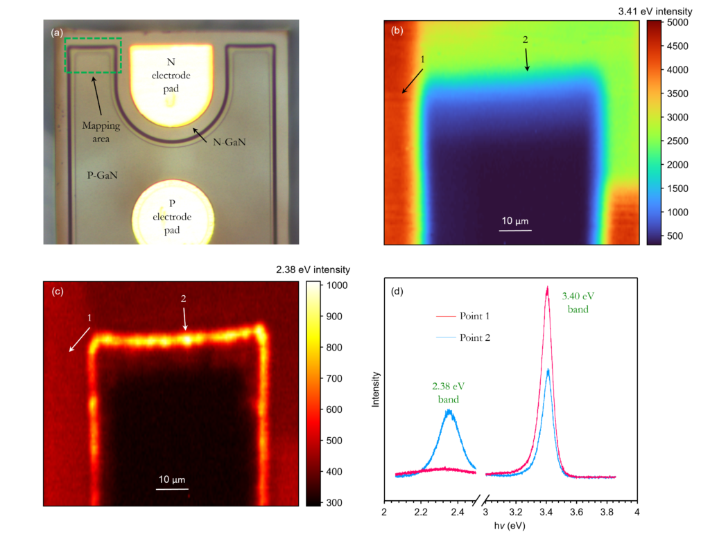
In our recent application note, we showed how the Edinburgh Instruments RMS1000 Confocal Microscope can be used to perform Raman and PL imaging on a GaN-based LED device, a picture of which is shown in panel (a) above. In this Map of the Month blog we highlight the information provided about the LED by PL imaging. PL directly measures bandgaps in semiconductors, and since bandgap energies are highly sensitive to impurities such as dopants and defects, microscopic analysis can yield detailed information about their presence. PL imaging was conducted on the region on the chip shown in panel (a) above, and false colour imaging was performed using UV and visible bands. Since GaN exhibits PL in the UV, a 325 nm He-Cd laser was required for excitation, which was externally coupled to the RMS1000.  

The UV (3.40 eV or 364 nm) PL intensity image in panel (b) above shows that the N-GaN exhibits PL, and the P-GaN does not. P doping of GaN using Mg has been shown previously to dampen the UV emission. The N-GaN region emits strongly except for a region in the top right-hand side of the image. In the application note, we demonstrated that this drop in UV PL was due to compressive strain in the N-GaN crystalline structure, which we probed using peak position Raman imaging.  

The visible band at 2.38 eV (520 nm) corresponds to PL from InGaN, the layer sandwiched between the P- and N-GaN that gives the LED its green colour. The image in panel (c) shows that this emission was largely confined to the black strip at the boundary of the P and N layers. The spectra in panel (d) show that the emission was more intense and blue-shifted from the weak visible emissions in the N-GaN layer.  

Read our full application note, Raman and Photoluminescence of Gallium Nitride to find out how Raman microscopy was also used to analyse this GaN-based LED.

RELATED PRODUCTS

RMS1000

Multimodal Confocal Microscope

VIEW

RESOURCES

Tags:
  • Map of the Month
  • RMS1000
  • Photoluminescence
  • Raman
Suggested Reading:

Raman and Photoluminescence Characterisation of GaN

View more »
Share:
PrevPrevious
NextNext

Keep up to date with the latest from Edinburgh Instruments

Join our mailing list and keep up with our latest videos, app notes and more!

LOCATION:
  • Edinburgh Instruments Ltd.
    2 Bain Square, Kirkton Campus, Livingston, EH54 7DQ.
  • sales@edinst.com
  • +44 1506 425 300
ABOUT:
  • About Us
  • Techniques
  • Applications
  • Knowledgebase
  • About Us
  • Techniques
  • Applications
  • Knowledgebase
PRODUCTS:
  • Fluorescence Spectrometers
  • Raman Microscopes
  • UV-Vis Spectrophotometers
  • Transient Absorption
  • FTIR Spectrometers
  • Lasers and LEDs
  • Customisation Options
  • Software
  • Upgrades
  • All Products
  • Fluorescence Spectrometers
  • Raman Microscopes
  • UV-Vis Spectrophotometers
  • Transient Absorption
  • FTIR Spectrometers
  • Lasers and LEDs
  • Customisation Options
  • Software
  • Upgrades
  • All Products
LEGALS:
  • News
  • Events
  • Blog
  • Careers
  • Contact Us
  • Terms and Conditions
  • Privacy Policy
  • News
  • Events
  • Blog
  • Careers
  • Contact Us
  • Terms and Conditions
  • Privacy Policy
SOCIALS:
Youtube Linkedin X-twitter Facebook
©2024 Edinburgh Instruments. Registered in England and Wales No: 962331. VAT No: GB 271 7379 37
Manage Consent
To provide the best experiences, we use technologies like cookies to store and/or access device information. Consenting to these technologies will allow us to process data such as browsing behaviour or unique IDs on this site. Not consenting or withdrawing consent, may adversely affect certain features and functions.
Functional Always active
The technical storage or access is strictly necessary for the legitimate purpose of enabling the use of a specific service explicitly requested by the subscriber or user, or for the sole purpose of carrying out the transmission of a communication over an electronic communications network.
Preferences
The technical storage or access is necessary for the legitimate purpose of storing preferences that are not requested by the subscriber or user.
Statistics
The technical storage or access that is used exclusively for statistical purposes. The technical storage or access that is used exclusively for anonymous statistical purposes. Without a subpoena, voluntary compliance on the part of your Internet Service Provider, or additional records from a third party, information stored or retrieved for this purpose alone cannot usually be used to identify you.
Marketing
The technical storage or access is required to create user profiles to send advertising, or to track the user on a website or across several websites for similar marketing purposes.
Manage options Manage services Manage {vendor_count} vendors Read more about these purposes
View preferences
{title} {title} {title}