Welcome to Edinburgh Instruments’ blog celebrating our work in Raman, Photoluminescence, and Fluorescence Lifetime Imaging. Every month, we aim to highlight our pick for Map of the Month to show how our Raman and fluorescence spectrometers can be used to reveal all the hidden secrets in your samples.

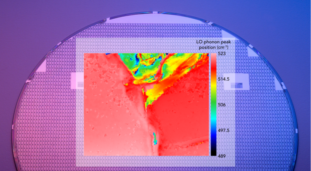
Semiconductors are a crucial part of modern life. They are used in every conceivable electronic device, enabling communications, computing, transportation, and healthcare advancements. Their role is to control and manage the flow of electric currents in such devices. Many different materials are classed as semiconductors, but the most commonly used is silicon because it is so abundant and cheap to use. Silicon must have the same properties within an electronic device at all points because the material’s properties are related to performance. Different levels of performance across a device can adversely affect reliability.
Raman microscopy can be used to track these properties and, therefore, is a great method for quality assurance in semiconductor manufacturing settings, see above. Here, we mapped a defective silicon semiconductor wafer and saw changes in the optical properties due to the defect. First, we saw shifts in the position of the prominent silicon peak. This suggests that the energy of that vibration varied across the wafer, which is typically associated with strain. When the same region was mapped using peak width, areas of nanocrystalline silicon were also detected. Read more about it in our Application Note: Raman Imaging of Strain in a Silicon Semiconductor Wafer.